
 5 hours ago
7
5 hours ago
7
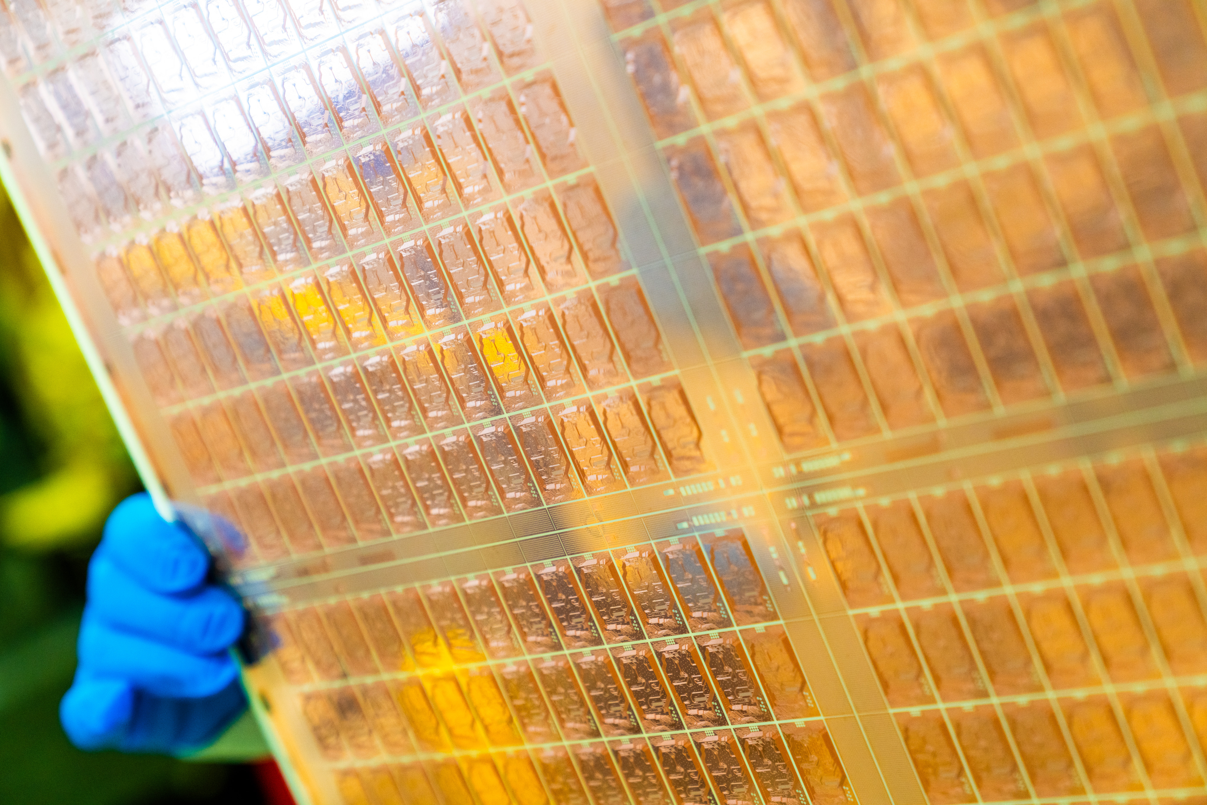
The race is on to build the massive chip packages that power the future of AI, with some technologies being developed to produce a single chip that houses a monstrous 58 chips in one unit. But the future pathway to those sorts of massive chips isn't entirely agreed upon yet, as learned at TSMC's recent European Technology Symposium that we attended.
Although panel-level packaging technologies are set to enable much larger chip packages, they will not provide, at least initially, the same interconnection densities as today's wafer-level packaging technologies like CoWoS, according to Kevin Zhang, TSMC’s senior vice president of business development and global sales and deputy co-COO.
"The geometry complexity panel-based process has to deal with is nowhere near the wafer level technology capability," Zhang said. "CoPoS, I would say it is one way to basically using panel-based process to continue driving the interposer scaling."
One of the common misconceptions in the semiconductor industry is that panel-based chip packaging technologies will replace existing wafer-based technologies like CoWoS as they promise to enable considerably larger package sizes — think 310mm×310mm, up from existing 120mm×150mm — at lower costs. This is not the case, though, according to TSMC.
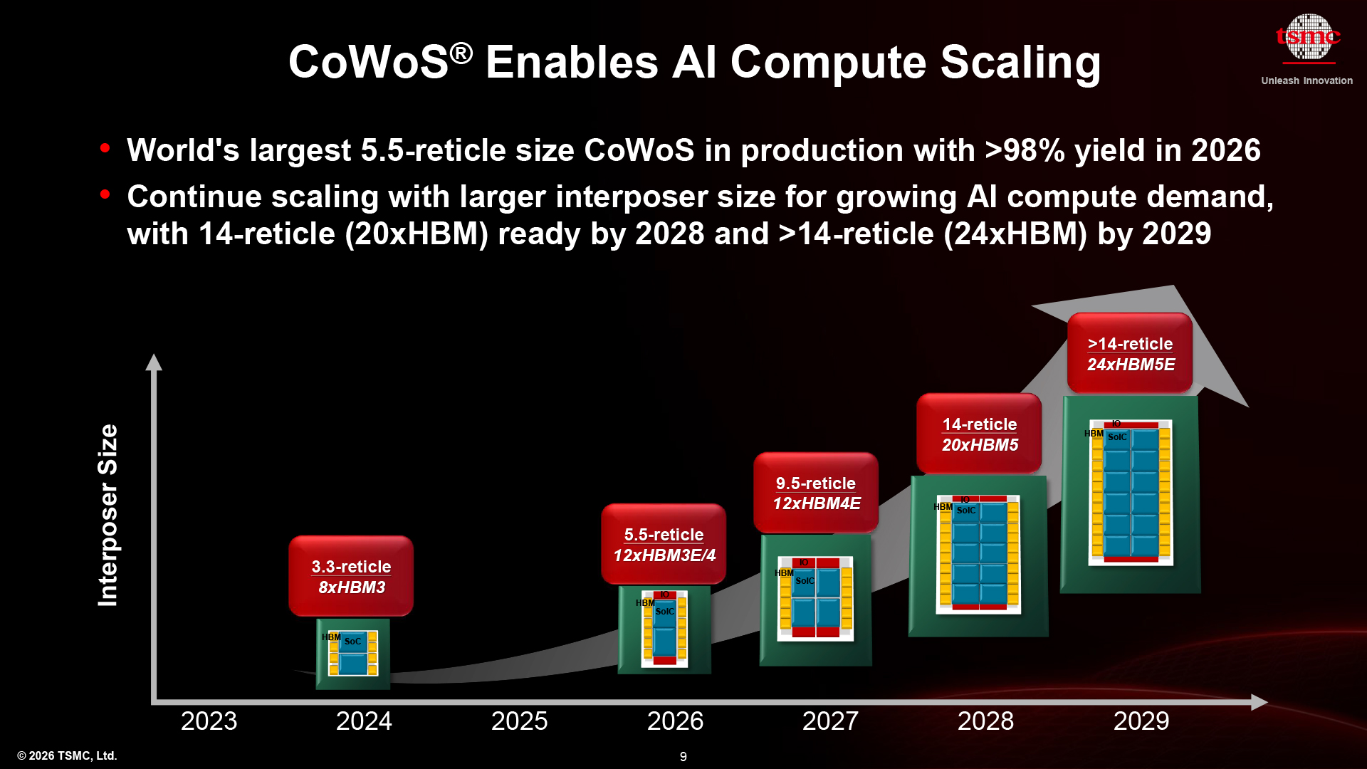
"That is an option on the table," Zhang said. "But remember, if you look at our CoWoS roadmap, we still have a lot of runway left with wafer-level technologies. We can scale CoWoS all the way to 14X using wafer-level processes, and we also have wafer-level integration. […] You can integrate 58 large reticle-sized dies together. So, there is still plenty of room for us to continue advancing wafer-level integration. At the same time, our team always wants to make sure we evaluate all future options. Obviously, one of those options is panel-based packaging."
But panel-level packaging cannot leverage the tools currently used for wafer-level packaging, as essentially technologies like CoWoS use the same lithography, etching, deposition, and other tools that were previously used to make logic chips. By contrast, panel-level integration tools are considerably less advanced.
"From technology point of view, wafer-level-based process is far more advanced than panel," Zhang said. "I am not talking about just TSMC, I am talking about the industry as a whole. Wafer-level processing is where the most advanced manufacturing technology exists today. To move to panel-based manufacturing, the industry needs to improve panel processes rapidly so they can eventually offer a better next-generation solution relative to wafer-level technology."
In fact, the main advantage that panels have over wafers is indeed larger package size: currently, TSMC can use 120mm×150mm substrates, next-generation CoWoS technologies will enable 150mm×250mm substrates, but even substrates the size of a hardcover book look pale compared to the initial 310mm×310mm panels. Furthermore, future packages can get to 515mm×510mm or even 750mm×620mm, which is larger than a wafer. When asked specifically whether CoPoS will complement CoWoS rather than replace it, Zhang essentially answered positively.
"I think that may be a way to look at it because it depends on the specific product configuration," Zhang said. "At some of the product will continue to get optimum benefit by leveraging wafer-level processing capability. Our goal is to offer our customer all the options they would need in order to find the optimum solution for their next-generation product. CoWoS today [has a lot of] scaling room for us to continue to drive this technology forward. But at the same time, we are looking at a fan-out-based process, some use the word CoPoS, as another alternative path going forward."
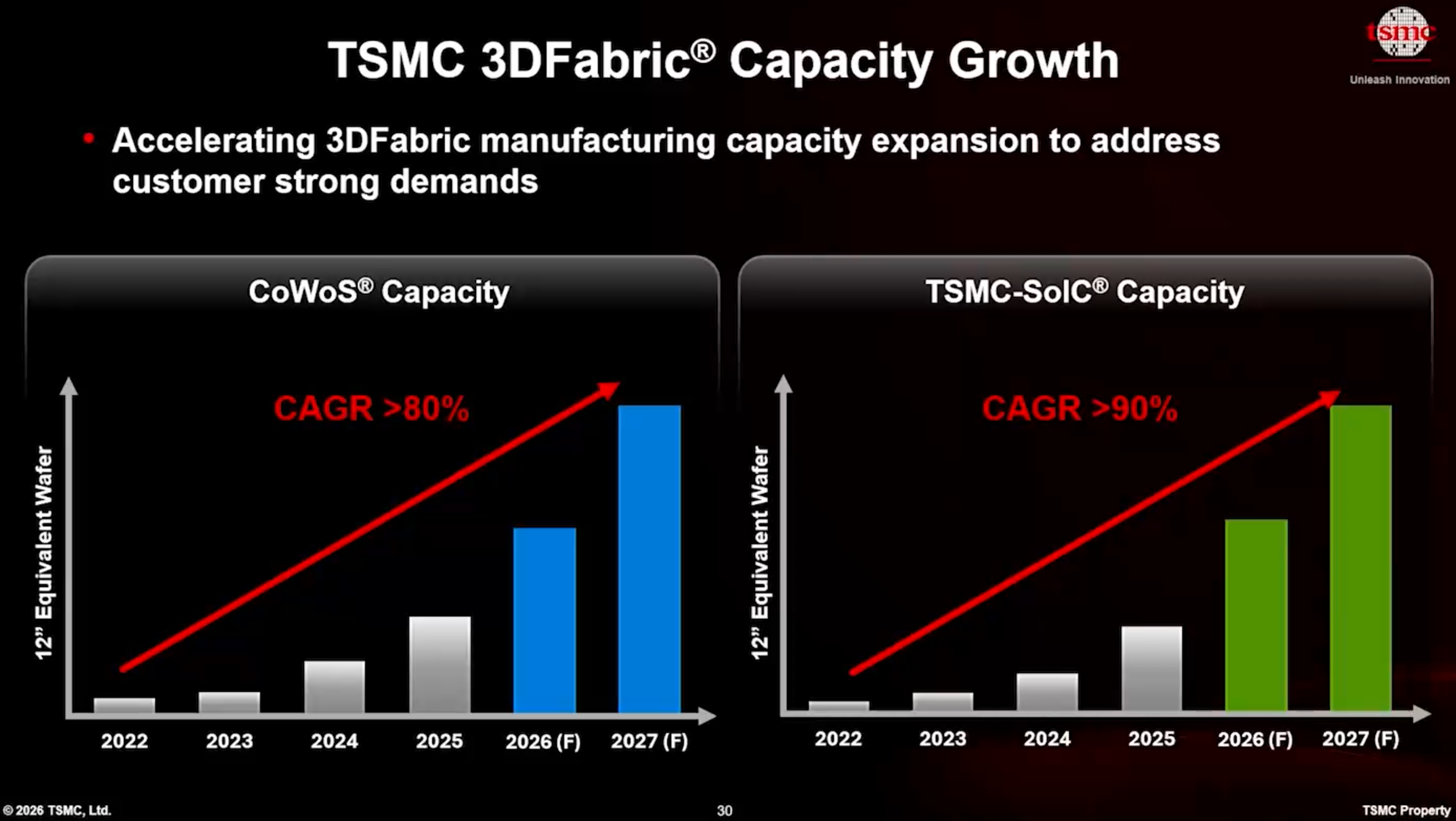
TSMC is currently expected to complete its first CoPoS pilot line this June. The gap between pilot and meaningful production is often around two or three years, so a reasonable expectation for high-volume manufacturing (HVM) using CoPoS would be 2028 – 2029. However, keeping in mind that CoPoS uses new tools and since the peculiarities of these tools are unknown, it is more reasonable to expect the first CoPoS-based products in 2029 or 2030, with more meaningful volumes sometime in the first half of the next decade. At the end of the day, CoWoS existed for years before explosive adoption, so CoPoS will likely repeat this pattern.

Follow Tom's Hardware on Google News, or add us as a preferred source, to get our latest news, analysis, & reviews in your feeds.


 English (US) ·