IBM and Lam Research team up on High NA EUV dry resist to push chip scaling past 1nm
4 weeks ago
22
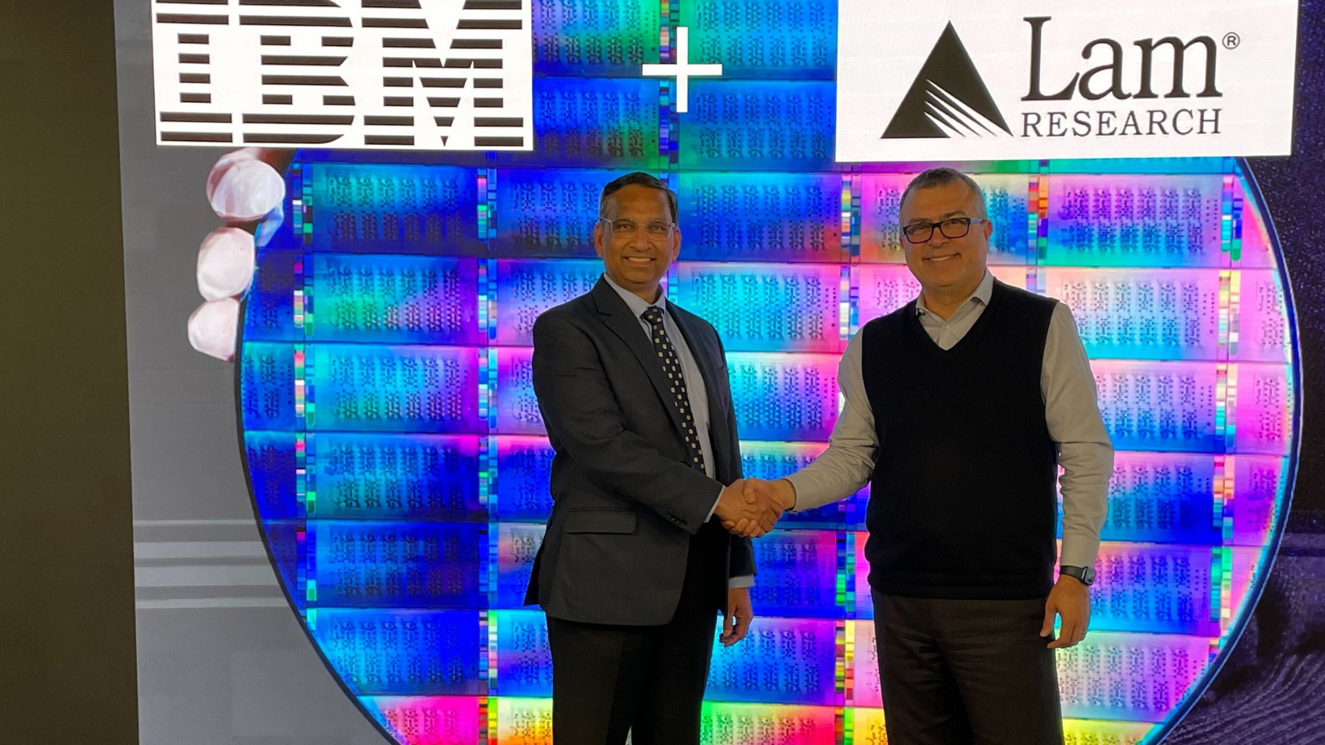
(Image credit: IBM Research)
IBM and Lam Research have announced a five-year collaboration to develop the materials and fabrication processes needed to scale logic chips beyond 1nm using High NA EUV lithography and Lam's Aether dry resist technology. The work will take place at IBM Research's facilities at the NY Creates Albany NanoTech Complex in Albany, New York.
The two companies have worked together for more than a decade, contributing to 7nm process development, nanosheet transistor architecture, and early EUV process integration, with IBM unveiling what it described as the world's first 2nm node chip in 2021 as part of that ongoing partnership. Under the new agreement, the focus will shift to validating full process flows for nanosheet and nanostack device architectures and backside power delivery, using Lam's Kiyo and Akara etch platforms, Striker and ALTUS Halo deposition systems, and Aether dry resist.
Conventional EUV lithography relies on chemically amplified resists, wet-process materials that struggle with the tighter tolerances demanded by high-NA EUV scanners. Meanwhile, Lam's Aether technology is a dry resist, deposited via vapor-phase precursors rather than spin-coating, and developed using plasma-based dry processes.
Article continues below
Aether’s metal-organic compounds absorb three to five times more EUV light than traditional carbon-based resist materials, which reduces the exposure dose needed per wafer pass and helps maintain single-print patterning at advanced nodes without resorting to more expensive multi-patterning. In January, Lam announced Aether had been selected by a leading memory manufacturer as the production tool of record for its most advanced DRAM processes, though it did not name the manufacturer.
According to the joint announcement, the collaboration seeks to enable High NA EUV patterns to be reliably transferred into real device layers at high yield, and to accelerate industry adoption of High NA EUV for next-generation interconnect and device patterning. That yield-at-transfer problem is where Lam's Aether dry resist technology has an edge over conventional wet processes, because fewer steps between exposure and etch mean less opportunity for pattern degradation at tighter geometries.
Meanwhile, nanosheet transistors stack multiple thin sheets of silicon to increase drive current without widening the device footprint. The press release confirms the teams will build and validate full process flows for both nanosheet and nanostack devices, alongside backside power delivery, which routes power through the back of the wafer to free up front-side interconnect layers for signal routing.
“Together, these capabilities are aimed at allowing High‑NA EUV patterns to be reliably transferred into real device layers with high yield and enabling continued scaling, improved performance, and viable paths to production for future logic devices,” says the press release.
Get Tom's Hardware's best news and in-depth reviews, straight to your inbox.
Luke James is a freelance writer and journalist. Although his background is in legal, he has a personal interest in all things tech, especially hardware and microelectronics, and anything regulatory.

 4 weeks ago
22
4 weeks ago
22


 English (US) ·