
 3 hours ago
8
3 hours ago
8
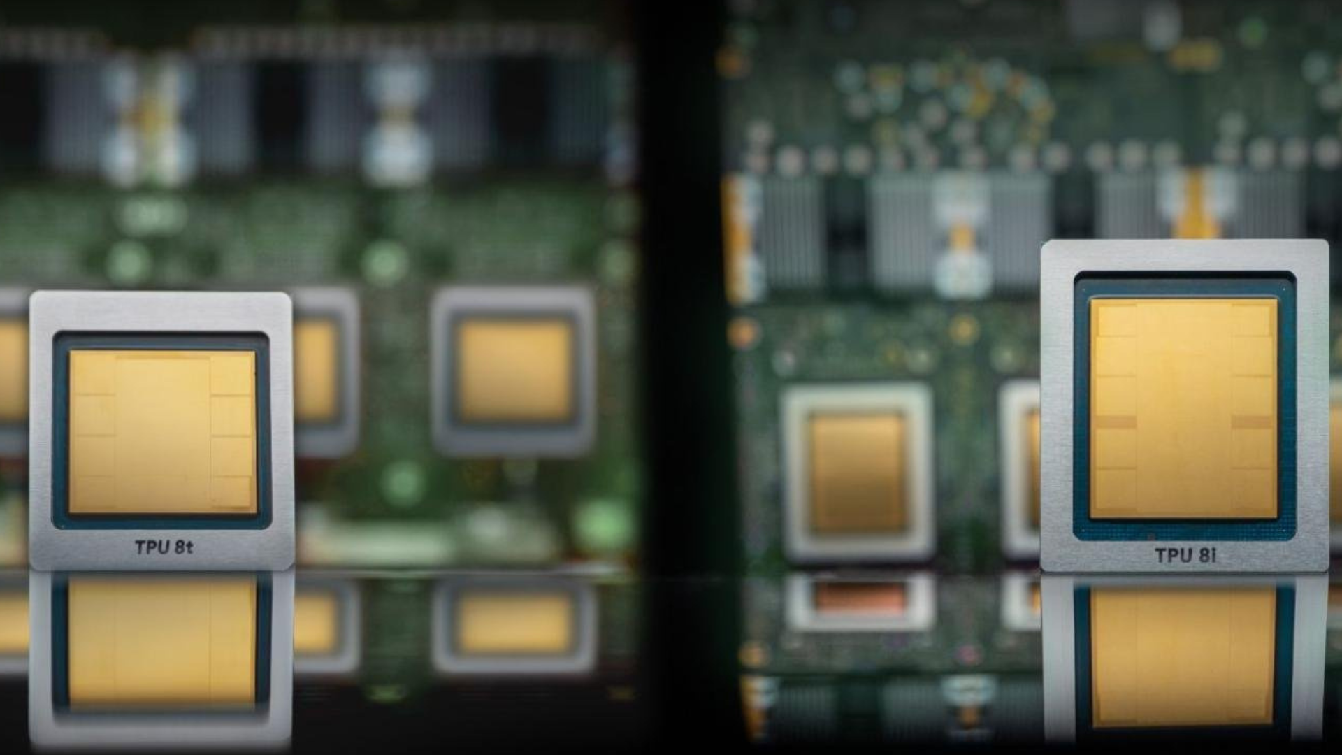
Google announced its eighth-generation Tensor Processing Units at Cloud Next on April 22, shipping two distinct chip designs for the first time in the TPU program's decade-long history. The two chips — TPU 8t and TPU 8i — are intended for use in different workloads. TPU 8t targets large-scale model training, while TPU 8i is built for low-latency inference and reasoning workloads.
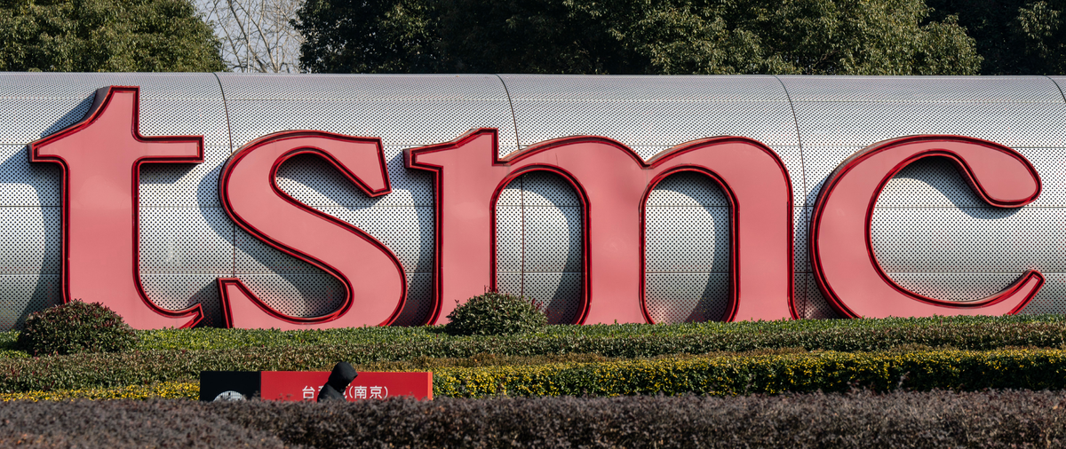
The split also extends to the supply chain, with MediaTek having joined Broadcom as a silicon design partner for the eighth-gen program back in December, ending Broadcom’s exclusive role in TPU development since 2015. Both chips are fabricated on TSMC's N3 process family with HBM3E memory and will be available to Google Cloud customers later this year.
Optionality for customers
In terms of raw specs, TPU 8 doesn’t close the gap with Nvidia or AMD. According to Google’s own technical deep dive, the TPU 8t delivers 12.6 FP4 PFLOPs with 216 GB of HBM3e running at 6,528 GB/s, while TPU 8i offers 10.1 FP4 PFLOPs, 288 GB of HBM3e at 8,601 GB/s, and 384 MB of on-chip SRAM. In comparison, Nvidia's Vera Rubin R200 is rated at 35 FP4 PFLOPs for training with 288GB of HBM4 at 22 TB/s, and AMD's MI455X reaches 40 FP4 PFLOPs with 432GB of HBM4. That makes the gap roughly 3:1 in raw compute per-socket.
Article continues below
Then there’s the choice of HBM3E over HBM4, which appears to be a deliberate cost and yield trade-off. TPU 8t carries 12.5% more memory capacity than the previous-gen Ironwood TPU, but delivers 11.5% less bandwidth, running slower memory to improve yield and bring down cost per chip per analysis from Next Platform. This is an odd strategy on the face of it, but it seems that Google, rather than trying to take on Nvidia in terms of raw performance, is creating options for external customers that want alternatives.
A TPU 8t superpod packs 9,600 chips into a single cluster with two petabytes of shared HBM, connected by a proprietary inter-chip interconnect running at double the previous generation's bandwidth. Google claims 121 FP4 ExaFLOPs from a single superpod, with the new Virgo Network fabric tying up to 134,000 TPU 8t chips into a single non-blocking data center fabric with 47 PB/s of bisection bandwidth, extending past 1 million chips across multiple sites.
So, yes, while individual Nvidia GPUs are faster, Google holds an advantage with its pod-level throughput at that mass scale; training workloads consume thousands of accelerators, not one, and Nvidia’s current-gen GPUs top out at 576 accelerators in a single NVLink deployment.
Interestingly, Google also announced Vera Rubin NVL72 instances running over the same Virgo Network fabric at Cloud Next, so TPUs are clearly not intended to act as a direct replacement for Nvidia silicon.
Swipe to scroll horizontally
| Row 0 - Cell 0 | TPU 8t | TPU 8i |
Workload | Large-scale pre-training | Sampling, serving, and reasoning |
Network topology | 3D Torus | Boardfly |
Specialized chip features | SparseCore (Embeddings) & LLM Decoder Engine | CAE (Collectives Acceleration Engine) |
HBM capacity | 216 GB | 288 GB |
On-chip SRAM | 128 MB | 384 MB |
Peak FP4 PFLOPs | 12.6 | 10.1 |
HBM bandwidth | 6,528 GB/s | 8,601 GB/s |
CPU header | Arm Axion | Arm Axion |
TPU 8i architecture
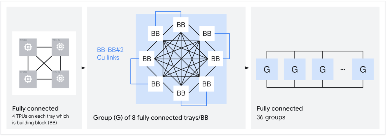
The TPU 8i’s architecture is a radical departure from the norm for Google, with TPU 8i abandoning the 3D Torus interconnect that has been inside TPU pods since the second generation. Instead, it’s replaced with a topology that Google calls “Boardfly,” inspired by the 2008 Kim/Dally Dragonfly paper. Boardfly is a three-tier hierarchy: four-chip building blocks connected into 32-chip groups by copper cabling, with 36 groups linked by optical circuit switches into a pod of up to 1,024 active chips.
In a 1,024-chip 3D Torus configuration, the worst-case packet path traverses 16 hops. Boardfly cuts that to seven, a 56% reduction in network diameter that directly benefits mixture-of-experts (MoE) models, where token routing requires frequent all-to-all communication across unpredictable chip pairs.
TPU 8i also replaces the SparseCore embedding accelerators that Google has used since TPU v4 with a new fixed-function block called the Collectives Acceleration Engine (CAE). The CAE offloads reduction and synchronization operations during autoregressive decoding, cutting on-chip collective latency by up to five times. Combined with the tripled SRAM, which holds more of the KV cache on-chip during long-context inference, Google claims 80% better performance per dollar over Ironwood for large MoE models at low-latency targets.
TPU 8t, meanwhile, retains the 3D Torus at a larger scale and keeps SparseCore for the irregular memory access patterns typical of embedding lookups during training. It introduces native FP4 compute to double MXU throughput at reduced precision, and a new TPUDirect RDMA path that bypasses the host CPU to pull data directly from high-speed managed storage, delivering what Google describes as ten times faster storage access over the previous generation. Both chips now run on Google's Arm-based Axion CPU hosts, replacing x86 for the first time.
Two suppliers instead of one
The MediaTek partnership means that there’s a second silicon design house in the TPU program alongside Broadcom, with MediaTek understood to be handling the design of the TPU 8i inference chip while Broadcom handles the design of the 8t training chip.
TrendForce reported back in December that MediaTek initially booked 20,000 TSMC CoWoS wafers for the program, with allocation potentially scaling to 150,000 by 2027. According to Bank of America analyst Vivek Arya, the dual-sourcing arrangement could reduce per-chip cost by up to 30% compared to solely sourcing from Broadcom, whose role is secured through at least 2031 per an April 6 SEC filing, which also formalized a 3.5 GW TPU capacity commitment from Anthropic starting in 2027. That deal sits on top of the one gigawatt of Anthropic capacity already coming online this year under a separate Google Cloud agreement.
Meanwhile, Meta has signed a separate multi-year, multi-billion-dollar TPU rental agreement, estimated to involve 500,000 to 800,000 TPU chips by 2027 if initial testing meets expectations, and Apple is routing Gemini-powered Siri workloads to Google Cloud on TPU infrastructure, valued at roughly $1 billion per year.


 English (US) ·