
 1 month ago
77
1 month ago
77
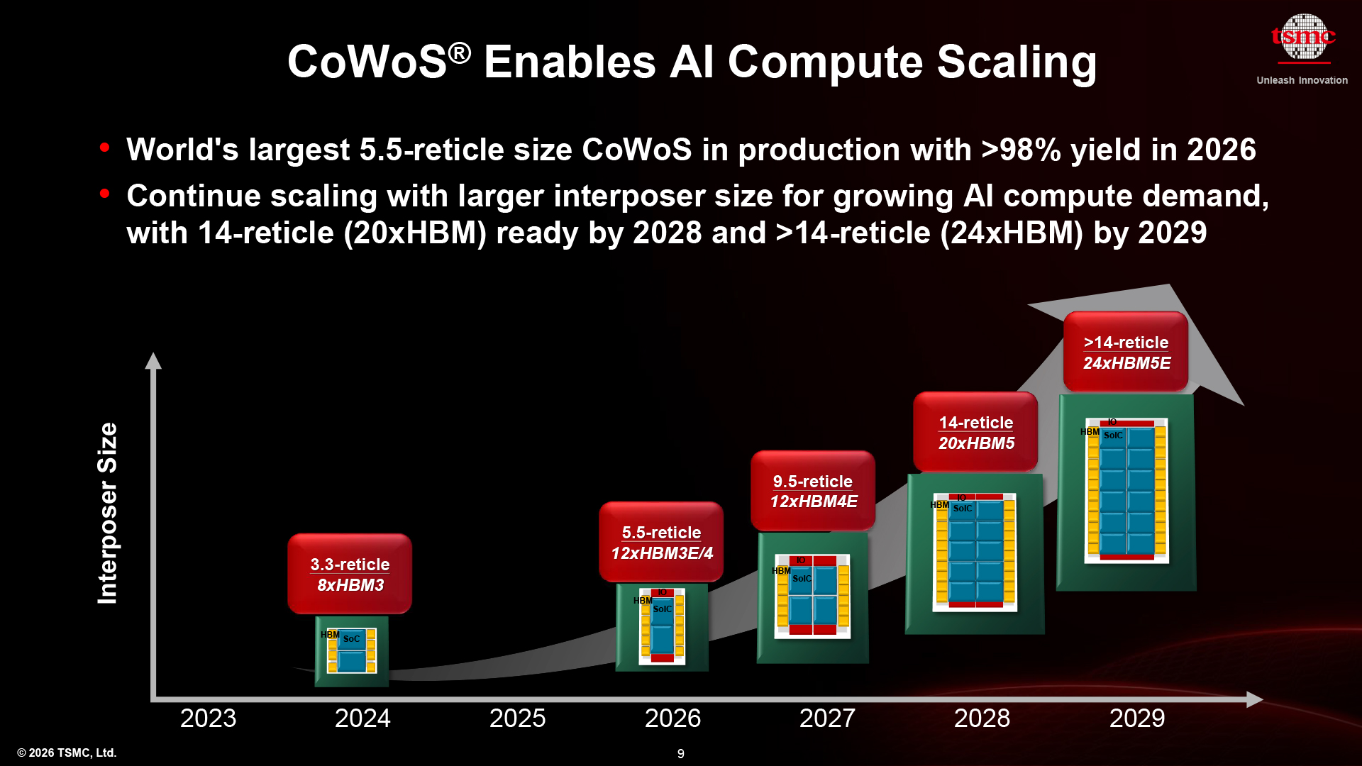
At the North American Technology Symposium 2026, TSMC revealed its updated CoWoS packaging roadmap with major enhancements. Within chipmaking, the reticle limit is the largest size that a chip can be printed within a single step of the manufacturing process. TSMC's previous CoWoS-based system-in-packages (SiPs) roadmaps topped out at a 9.5-reticle size.
Now the company expects to produce 14-reticle and over 14-reticle-sized System-in-Packages (SiPs) with up to 24 HBM5E stacks by 2029. Such high integration is designed to meet the insatiable demand that AI accelerators have for both compute and memory bandwidth, and signals that packaging, not lithography, acts as a primary driver for semiconductor technologies.
Article continues below
Bigger, hotter and hungrier
It is common for contemporary process technologies to scale slowly in transistor density, while full-node scaling enables 15% to 20% higher transistor density every three years. Intra-node improvements yield diminishing returns in density, but continue to provide performance improvements and greater power efficiency. This may not be a big problem for consumer product-makers, but it greatly affects the developers of AI and HPC applications, who must improve their solutions every year or two to remain competitive.
For those customers, TSMC has begun mass production of 5.5-reticle-sized CoWoS SiPs, supporting up to 12 HBM3E/HBM4 stacks and has achieved yields over 98%, according to the company.
In 2027, TSMC's CoWoS roadmap outlines a 9.5-reticle-sized interposer that supports 12 HBM5 stacks, which is expected to require a 120 mm by 150 mm substrate. In 2028, the company expects to produce a 14-reticle-sized interposer capable of carrying 20 3D-stacked compute chiplets and 20 HBM5 modules. By 2029, TSMC expects to produce interposers over 14 reticle sizes, with up to 24 HBM5E stacks. One standard reticle measures 26 mm by 33 mm (858 mm2), so a 14-reticle-sized interposer measures 12,020 mm2, or the size of a small plate, and slightly larger than a CD.
An SiP that uses a 14-reticle-sized interposer and measures 12,020 mm2 will consume an enormous amount of power, will require an exotic cooling solution (think exotic cold plates like those developed by Frore Systems, immersion cooling, or a combination of both), and will require a massive substrate, which will occupy a significant share of a server motherboard's real estate. The dimensions of the SiP alone will redefine how AI servers are built, whereas power consumption and cooling requirements are poised to open doors to a host of new technologies.
48x more compute transistors, 34x more bandwidth by 2029
Such gargantuan multi-chiplet processors show that advanced packaging is now the de facto scaling engine for the industry. In fact, TSMC's lateral CoWoS and vertical SoIC technologies enable faster growth of transistor budgets than traditional Moore's Law scaling. In addition, such SiPs also offer more memory bandwidth.
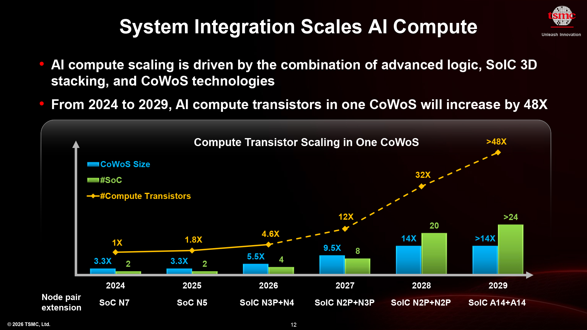
Based on TSMC's expectations, its customers will be able to put (at least) as many as 24 3D-stacked compute chiplets on one 14 reticle-sized CoWoS interposer by 2029, when A14 will be in mass production. When combined with scaling enabled by the latest process technologies (4x from N7 to A14), an ultra-high-end SiP from 2029 with 24 3D-stacked A14-based chiplets will be able to carry 48x more compute transistors than a high-end SiP with two N7-based chiplets from 2024, according to TSMC. Granted, we've rarely seen frontier dual-chiplet N7-based SiPs in 2024, even a cautious Nvidia opted to use 4NP instead.
There is a catch regarding 3D-stacked compute transistors, though. The bottom die may overheat, whereas the top die must get enough power to reach its full potential. To that end, many designs use the bottom die for cache (e.g., AMD's Zen 5-based CPUs with 3D V-Cache), not for compute.
Nonetheless, even a 24x increase in the number of compute transistors per high-end SiP in five years is a breakthrough that could not be achieved by Moore's law alone. However, such integration comes at a price. In the 2030s, cutting-edge SiPs with 24 3D-stacked compute chiplets and 24 HBM5E modules will likely cost an order of magnitude more than a high-end SiP from the mid-2020s.
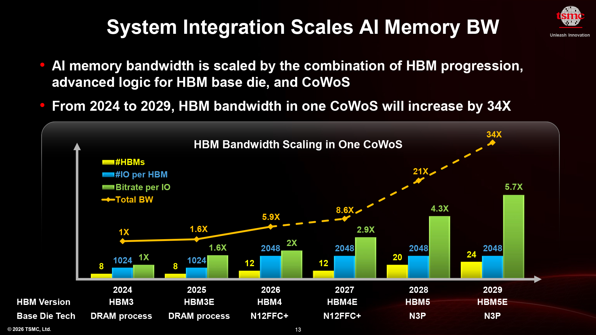
In addition to compute capability, large CoWoS interposers also enable considerably higher memory bandwidth simply because they can carry more HBM stacks. It is not that simple, though. Total memory bandwidth scales dramatically, driven by the combination of wider HBM4 and HBM5 interfaces, more advanced HBM base dies built on TSMC’s N3P process, and ongoing CoWoS improvements that enable faster interconnect speeds. As a result, a high-performance SiP integrating 24 HBM5E stacks in 2029 is expected to deliver up to 34x higher bandwidth when compared to a reference SiP with eight HBM3 stacks in 2024, according to TSMC.
"HBM bandwidth scaling comes from multiple factors," said TSMC. "First, there is the memory itself — progressing from HBM3 to HBM4, with higher I/O counts. In addition, we are leveraging more advanced logic technologies for the base die, which allows us to push data rates well beyond 10 Gb/s per pin, something that was unheard of in traditional DRAM. At the same time, our CoWoS technology enables integration of more HBM stacks within a single package. […] All of these factors together — higher data rates, more I/O, and more stacks — contribute to the overall bandwidth scaling."
Slower transistor scaling
One of the things that strikes the eye about the current and upcoming process technologies due later this decade is the slow scaling of transistor density. While A14 is set to increase per-chip transistor density by 20% compared to N2 technology in 2028, its optical-shrink successor (A13) is only poised to provide a 6% higher density a year later.
Fortunately, TSMC continues to aggressively develop its CoWoS packaging technology, which promises to enable developers of system-in-packages to put 24 3D-stacked compute chiplets and 24 HBM5E modules onto one massive 14 reticle-sized interposer before the end of the decade. This will increase compute transistor count and memory bandwidth per SiP by 48x and 34x, respectively, compared to high-end data center SiPs in 2024, according to TSMC.
However, this level of integration will likely come at a high cost. System-in-packages with up to 24 3D-stacked compute chiplets and 24 HBM5E stacks in the 2030s will probably cost an order of magnitude more than high-end SiPs from the mid-2020s.


 English (US) ·