
 3 weeks ago
58
3 weeks ago
58
IMEC has successfully demonstrated the full wafer-scale fabrication of nanopores using ASML’s state-of-the-art extreme ultraviolet (EUV) machines. Described by ASML’s communications chief as an “unexpectedly awesome biomedical application,” of his firm's machinery, this could be an important advance due to the molecular sensing possibilities nanopores open up.
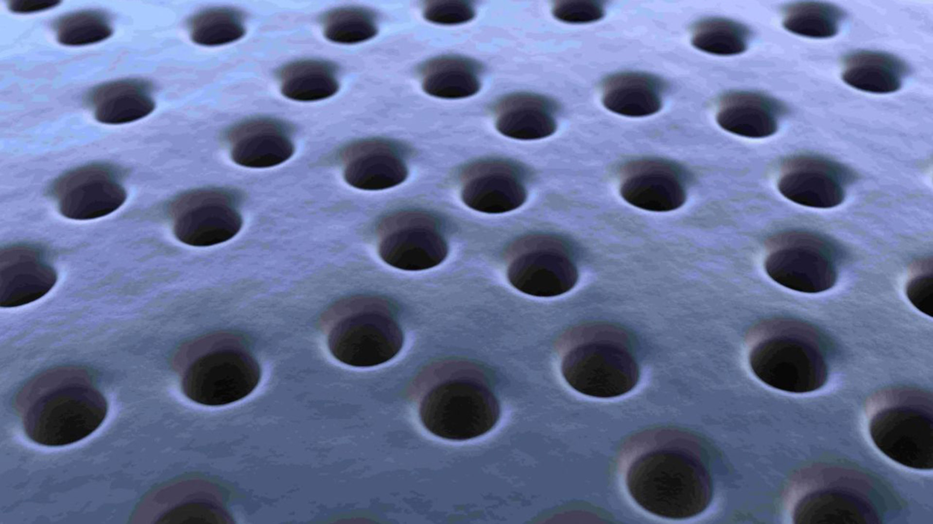
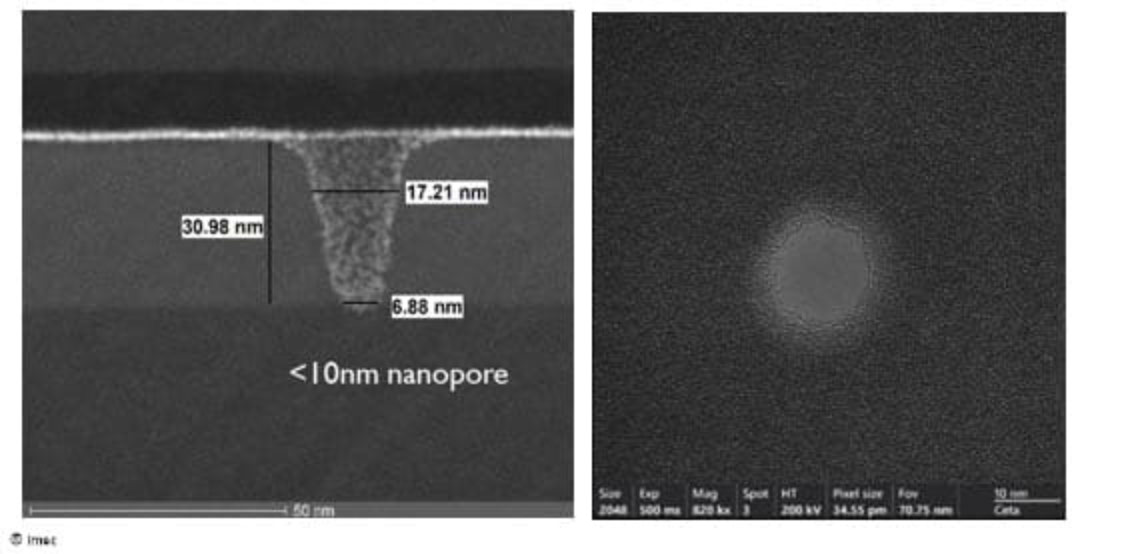
The qualities of nanopores are of great interest in biomedicine. As you might have determined from the etymology, nanopores are essentially tiny holes, just a few nanometers wide. In more relatable language, perhaps, these pores have diameters that make them roughly 10,000 times finer than a human hair.
What is the use of such tiny perforations?
Nanopores can be used by biomedical sensors due to the way molecules interact with them. The science behind their use in detection is:
- An ionic current flowing through the nanopores is measured,
- As molecules pass through, they create modulations giving away their size, structure, charge, and interactions,
- Different molecules can thus be detected from their distinct electrical signatures, with high sensitivity.
In this way, these EUV fabricated nanopores can act like molecular checkpoints for biomedical sensing. They can detect and determine individual molecules like a virus, protein, or DNA etc. That’s a great feature for accurate molecule identification and analysis. Furthermore, adjusting the solid state nanopore size can also be useful for filtration and molecular data storage applications, indicates IMEC.
Why use EUV machinery?
Current nanopore production methods are claimed to be slow, limited to the lab, and expensive. IMEC’s paper describes how it successfully fabricated “highly uniform nanopores with diameters down to ~10nm across full 300mm wafers.” This breakthrough – encompassing mass production, precision, and reproducibility - should put an end to the delays in adoption of nanopore-based sensors.
While we applaud the research, and the idea of making precision nanopores more accessible to medical equipment makers, we also understand that ASML EUV equipment isn’t that easy to acquire. Such is the demand for this high-tech machinery by the booming semiconductor industry, we hope there remains some chance for biomedical production runs like nanopore production.
However, we are slightly reassured by the researchers highlighting that this is a step towards “cost-effective (mass) production,” as surely they will have assessed the costs of getting a 300mm wafer full of nanopores produced at this time.

Follow Tom's Hardware on Google News, or add us as a preferred source, to get our latest news, analysis, & reviews in your feeds.


 English (US) ·