
 3 hours ago
3
3 hours ago
3

A team of researchers from the Institute of Science Tokyo unveiled a hardened wireless receiver that can withstand prolonged exposure to radiation at the IEEE International Solid-State Circuits Conference (ISSCC) in San Francisco, California, last February. According to the IEEE Spectrum, this chip was primarily designed to allow robots to work in contaminated areas for decommissioning nuclear reactors. Regular silicon-based semiconductors used for wireless communication are susceptible to interference from nuclear radiation, meaning robots are limited by the physical cable needed to control them.
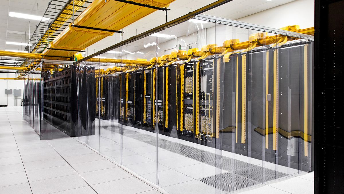
This became apparent during the cleanup at the Fukushima Daiichi nuclear plant, which suffered from a meltdown after the 2011 Tohoku earthquake and tsunami knocked out the plant’s backup energy sources required for cooling it. The robots tasked to clean up the contaminated areas required LAN cables to communicate with their operators, leading to tangled wires and making the operation more complicated than it already is.
Now, you cannot just get a consumer-grade Wi-Fi chip, chuck it in lead shielding, and call it a day to address the issue. After all, while shielding will stop radioactive emissions from hitting your chip, it will also block radio frequency signals. And while you might think that an antenna connected via a cable might solve the problem, that’s still not possible, as the antenna itself would be susceptible to radiation. That’s why the researchers decided to build a hardened Wi-Fi chip receiver that can withstand the radiation found in nuclear cores.
Article continues below
To understand how robust the chip needs to be, a robot operating in the environment of a nuclear reactor is exposed to a radiation dose of 500,000 grays (Gy, a unit to measure radiation dosage) over six months — by comparison, electronics installed in spacecraft must only withstand 100 to 300 Gy over a span of three years. The researchers achieved this by reducing the number of transistors inside the chip, as the oxide layer inside these semiconductors is susceptible to gamma rays. They replaced these instead with elements that don’t have an oxide layer, like inductors.

Follow Tom's Hardware on Google News, or add us as a preferred source, to get our latest news, analysis, & reviews in your feeds.


 English (US) ·