Intel's fab roadmap examined — Arizona, Ohio, Ireland, and the two deadlines deciding 14A process node
12 hours ago
44
(Image credit: Getty / Future Publishing)
This roadmap provides an in-depth analysis of Intel's current plans for its chip production capacity. In the space of 12 months, Intel has gone from canceling fabs to running short of them. In July last year, the company scrapped a planned €30 billion megafab in Magdeburg, Germany, and a $4.6 billion assembly and test plant near Wroclaw, Poland, citing a lack of committed demand. Then, in April this year, it paid Apollo $14.2 billion to repurchase the 49% stake in its Ireland fab that it had sold for $11.2 billion in 2024. Three weeks later, CFO David Zinsner described "unprecedented demand for silicon" alongside Q1 results that sent the stock up 24% in a single session, its best day since October 1987.
The next round of capacity development now hinges on two key deadlines: CEO Lip-Bu Tan told investors in January that prospective 14A customers will begin to make firm supplier decisions "starting in the second half of this year and extending into the first half of 2027." Separately, the enhanced 35% advanced manufacturing investment credit signed into law last July applies only to fab construction that begins before December 31st, 2026; projects that break ground in 2027 get nothing.
Both clocks run out within months of each other, and both bear on the same construction projects.
Swipe to scroll horizontally
Site
Fab
Node(s)
Status
Chandler, AZ
Fab 52
Intel 18A
Operational, ramping since October 2025
Chandler, AZ
Fab 62
Unassigned; 18A-capable
Under construction, ready around 2028
Hillsboro, OR
D1X
18A volume, 14A development
Operational; 14A volume targeted for 2028
New Albany, OH
Mod 1
14A and future nodes
Construction; operations 2030 to 2031
New Albany, OH
Mod 2
14A and future nodes
Construction; operations 2032
Leixlip, Ireland
Fab 34
Intel 4, Intel 3
Operational; wholly Intel-owned since April 2026
Kiryat Gat, Israel
Fab 38
Was slated for 18A-era expansion
Paused since mid-2024
Magdeburg, Germany
Two planned
Was slated for 14A-era nodes
Cancelled July 2025
Wroclaw, Poland
Assembly and test
N/A
Cancelled July 2025
Row 10 - Cell 0
Row 10 - Cell 1
Row 10 - Cell 2
Row 10 - Cell 3
Arizona
Fab 52 at the Ocotillo campus in Chandler is the production foundation for everything on Intel's 2026 to 2028 product roadmap. The facility became fully operational in October last year as the first high-volume home of Intel 18A, building Panther Lake compute tiles and, later this year, Clearwater Forest. Naga Chandrasekaran, Intel's chief technology and operations officer, told CNBC in December that the fab is "capable of more than 10,000 18A wafer starts per week," which works out to roughly 40,000 wafer starts per month at full ramp and makes it larger than TSMC's Fab 21 phase 1 and phase 2 combined.
That’s named capacity, however, not current output; Intel has indicated that 18A yields will reach industry-standard levels in early 2027, and until then, the company is capping CPU output on the node, leaving part of Fab 52's capacity idle. Tan said in May that 18A yields are improving by 7% to 8% per month.
Fab 62, the second from Intel's $20 billion 2021 Arizona expansion, is expected to be ready around 2028. Intel hasn’t officially assigned it a node, leaving it open as a stopgap for 14A if Ohio isn't ready, or as additional 18A capacity if external demand comes sooner. Brookfield Infrastructure put up to $15 billion into the two Chandler fabs in 2022 for a 49% share of the joint venture, and unlike the Apollo arrangement, Intel has made no move to buy that stake back, so every wafer out of Fab 52 and Fab 62 will have revenue share commitments attached to it.
Oregon
As the home of 14A, D1X complex at Gordon Moore Park in Hillsboro — a low-volume fab and development site — is currently the only place Intel develops leading-edge process technology, with Chandrasekaran telling CNBC the node will be developed first in Oregon, with a goal of risk production in 2028 and high-volume manufacturing in 2029.
Hillsboro houses Intel's High-NA EUV machines, including the first ASML Twinscan EXE:5200B system delivered anywhere, and 14A is the first Intel node designed around it. Oregon also carried early 18A production while Arizona ramped up. Intel began permitting work in February 2024 for a multibillion-dollar expansion of the campus following the approval of an air quality permit, though no construction start has been announced to date.
Ohio One
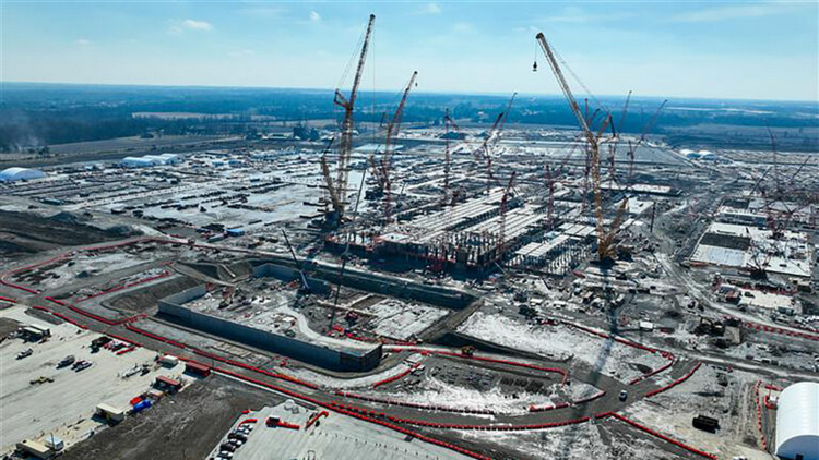
Ohio is Intel’s most problematic fab project on paper. It broke ground in New Albany way back in 2022 on a $28 billion first phase, originally targeting 2025 production. In February 2025, however, Chandrasekaran reset its schedule, targeting 2030 for the completion of Mod 1 with operations between 2030 and 2031, and Mod 2 in 2031 with operations in 2032. In a memo setting out this new schedule, Chandrasekaran said Intel preserves “the flexibility to accelerate work and the start of operations if customer demand warrants.”
An aerial view from February 2025 shows construction progress at Intel's Ohio One campus, where Intel plans to invest more than $28 billion in the construction of two new leading-edge chip factories. (Image credit: Intel Corporation)
Spanning nearly 1,000 acres, the site is designated for 14A and future nodes, and has room for up to eight fabs. Intel has spent roughly $5 billion there to date as of March 2025, including $1.4 billion in total for that year. Bechtel, the lead contractor, posted a wave of new construction job listings in January, the same month Tan declared Intel is “going big time into 14A.”
Still, customers (or a lack thereof) remain the gating factor for 14A production. Intel told investors in January that it’s got two prospective customers evaluating 14A test chips, and its SEC filings still warn that without a significant external customer, it “may pause or discontinue” 14A, successor nodes, and various manufacturing expansion projects.
Elon Musk said in April that his planned TeraFab project — the first named taker for the node — will use 14A process technology to make AI chips, though test production is expected to be years out. This also isn’t such a big win in terms of the volume commitment Intel’s filings say it needs for 14A to be viable. At the time of writing, 14A’s next and arguably most critical milestone is the 14A v0.9 PDK, which Tan says will reach external customers in October.
"The Holy Grail is v0.9 PDK. Right now, we are looking at October to [hand it to] the outside customer. Internal customer will be earlier, so that we make sure that we really clean the pipe, make sure that we are doing right, make sure that we can sell with good quality."
Ireland and canceled projects
Launched in 2023, Fab 34 in Leixlip is Intel's only EUV-class site in Europe, producing Intel 4 and Intel 3 silicon for Core Ultra and Xeon 6 parts. In 2024, Apollo-managed funds paid $11.2 billion for a 49% interest in the joint venture entitled to the fab's output, a deal that gave Intel a much-needed cash injection at the time.
In April this year, Intel bought that stake back for $14.2 billion — at a premium of roughly 27% — funded from cash and about $6.5 billion in new debt issuance. Apollo walked away with around $3 billion in return for two years of exposure, and Intel paid a nine-figure annual cost of capital to reclaim needed wafer revenue.
“Flexibility and alignment are core to how we approach relationships as a long-term, solutions-oriented capital partner, and we are pleased to facilitate this transaction in support of Intel's evolving strategic and operational priorities,” said Apollo Partner Jamshid Ehsani at the time.
Magdeburg, once pitched as a €30 billion home for 14A-era production with roughly €10 billion in German subsidies attached, was postponed to 2029-2030 in November 2024. This prompted the German government to reallocate those subsidies to the federal budget and, following a $3.2 billion operating loss with Q2 2025 financial results, Intel killed the project, the subsidies dying with it.
Wroclaw's $4.6 billion assembly and test plant was canceled the same day, and Costa Rica's assembly and test operations were consolidated into Vietnam and Malaysia. Fab 38 in Kiryat Gat, Israel, the planned $25 billion expansion announced in 2023 with $3.5 billion in Israeli government backing, has been paused for the last two years, with no restart announced. Every leading-edge wafer Intel produces for the foreseeable future will come therefore come from three U.S. states and one campus in Ireland.
Packaging and test
Fab 9 in Rio Rancho, New Mexico, a $3.5 billion conversion that opened in January 2024, is the only high-volume Foveros 3D stacking site in the United States. Foveros is the packaging behind every tiled Intel design since Meteor Lake, bonding compute, graphics, and I/O dies vertically rather than laying them side by side, and it is integral to the stacked Clearwater Forest parts now ramping on 18A.
Intel runs it alongside the neighboring Fab 11x as a single co-located operation, which EVP Keyvan Esfarjani called “the only U.S. factory producing the world's most advanced packaging solutions at scale.” The buildout created hundreds of Intel jobs and more than 3,000 construction roles, and the campus later drew a further $500 million in CHIPS funding for modernization.
The $7 billion Penang complex in Malaysia, placed on indefinite hold in early 2025, has been revived: the buildout is now 99% complete, and first-phase assembly and test operations are due to begin later this year, according to Malaysian Prime Minister Anwar Ibrahim, following an earlier briefing with Tan. Intel has also outsourced EMIB production to Amkor's Songdo facility in South Korea, and its next-generation EMIB-T packaging rolls out across production fabs this year.
With Magdeburg and the Penang delay having stripped packaging options elsewhere, Rio Rancho is now the load-bearing U.S. node for the back-end work that makes Intel's entire chip roadmap possible.
Two deadlines and three things to watch
Intel’s 14A commitment window and the cutoff for tax credits both converge in the second half of this year. Tan’s stated expectation is that customers make firm supplier decisions between the second half of 2026 and the first half of 2027, with results from the upcoming October PDK potentially being the trigger for those decisions.
On June 8th, Cadence announced a multi-year agreement with Intel Foundry to co-optimize designs for 14A and deliver production-ready process design kits. This is exactly the EDA groundwork that needs to be in place before any fabless customer can commit volume, and a committed volume customer will be what unlocks acceleration at Ohio and gives Fab 62 a job. The alternative, per Intel, is to cancel 14A altogether.
Unlike the customer deadline set by Intel, the tax deadline can’t slip. The so-called One Big Beautiful Bill Act raised the Section 48D advanced manufacturing investment credit from 25% to 35% in July last year, but the law's termination clause is unchanged: the credit doesn't apply to “property the construction of which begins after December 31, 2026.”
Treasury rules let a physical-work test or a 5% spend safe harbor establish a construction start, so Intel has roughly six months to break ground on any new shells, in Ohio, Arizona, or Oregon, that it wants the U.S. government to part-fund. The government, of course, has been a shareholder since August, when $5.7 billion in unpaid CHIPS grants from Intel's $7.86 billion award and $3.2 billion in Secure Enclave funds were converted into a 9.9% equity stake.
Ultimately, we’re going to be watching for three things before January: a named 14A customer with a volume commitment; a construction-start announcement timed to beat the credit deadline; and 18A yield milestones that free up the Arizona capacity Intel’s currently sitting on.
Luke James is a freelance writer and journalist. Although his background is in legal, he has a personal interest in all things tech, especially hardware and microelectronics, and anything regulatory.

 12 hours ago
44
12 hours ago
44


 English (US) ·