
 1 day ago
15
1 day ago
15
Intel CFO Dave Zinsner told the Morgan Stanley TMT conference last month that Intel Foundry is "close to closing some deals that are in the billions per year in terms of revenue" on advanced packaging alone, with EMIB-T, the next-generation variant of Intel's embedded bridge technology, driving customer interest as TSMC's CoWoS-L capacity remains structurally oversubscribed.
That tech, EMIB-T, which adds through silicon vias (TSVs) to the bridge, is expected to enter production fab rollout this year and addresses the limitations that have kept standard EMIB out of high-power AI accelerator sockets: HBM 4 class power delivery and large package scaling.
If these “billions per year” in deals close, it’d mark quite the turnaround for Intel Foundry, which generated just $307 million in external revenue last year against a $10.3 billion operating loss. Given that 18A isn’t expected to reach industry-standard yields until next year at the earliest, packaging is the fastest on-ramp for Intel, and EMIB-T is what could convert that into AI accelerator revenue. Intel Foundry's most recent announcement aligns well with this, having signed up to join Musk's Terafab project, though the reality of the effort delivering on all that's been promised remains extremely optimistic, as we've broken down.
Article continues below
EMIB-T and PSVs
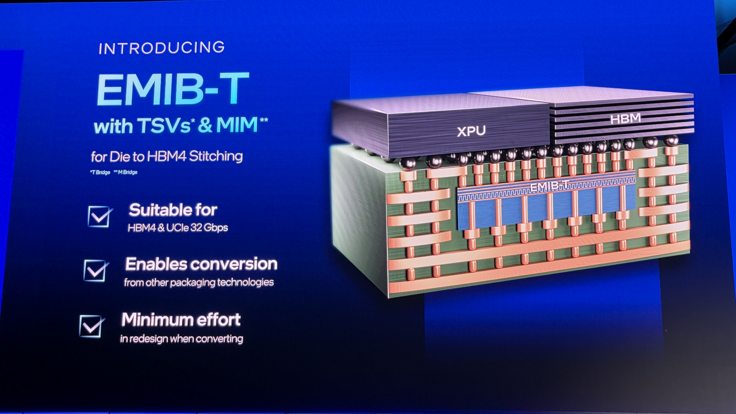
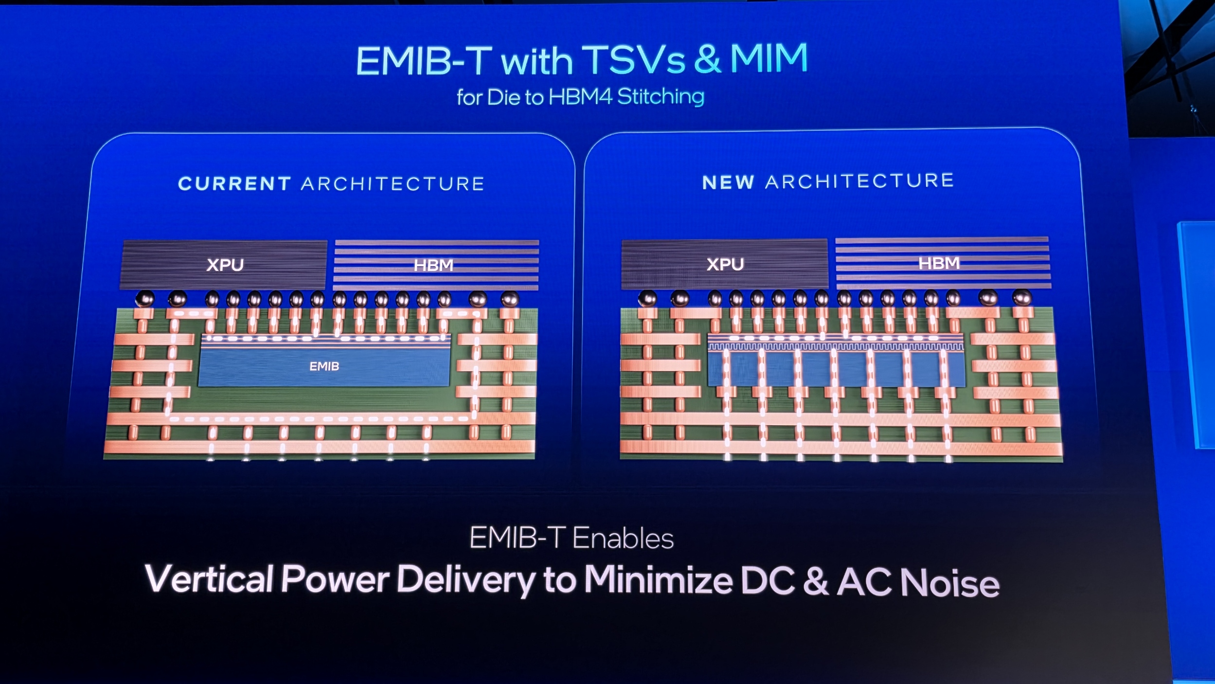
Standard EMIB, which has been in volume production since 2017, embeds small silicon bridge dies in cavities within an organic substrate to route signals horizontally between adjacent chiplets, avoiding the cost and reticle limits of a full silicon interposer.
Intel deliberately skipped through-silicon vias entirely with EMIB, keeping the bridge die simple and cheap. That meant power had to be routed around the bridge via the organic substrate in long, resistive paths, limiting the current that could be delivered to the dies above. That ceiling was fine for the likes of Sapphire Rapids and Ponte Vecchio, but not for HBM4-class accelerators.
EMIB-T reverses that decision by adding through-silicon vias (TSVs) to the bridge die. In doing so, EMIB-T enables vertical power delivery directly through the bridge, integrates Metal-Insulator-Metal capacitors for noise suppression, and adds a copper ground plane grid for signal isolation.
Dr. Rahul Manepalli, Intel Fellow and VP of Substrate Packaging Development, gave us a look into the full specifications of EMIB-T at last May’s Electronic Components Technology Conference — a 45-micron bump pitch with a roadmap to 35- and 25-micron, energy efficiency of around 0.25 pJ/bit, and UCle-A interfaces running at 32 Gb/s of data transfer or higher per pin. EMIB-T supports HBM3, HBM3E, HBM4, and future HBM5 stacks, and scales to a 120mm x 180mm package supporting more than 38 bridges and over 12 reticle-sized dies.
Intel then followed up just before Christmas with a conceptual 2.5D/3D package integrating 16 compute elements across eight base dies, 24 HBM5 stacks, and a 10,296 mm2 silicon footprint, scaling to 12x reticle size and beating TSMC's planned 9.5x CoWoS-L ceiling. For comparison, TSMC's CoWoS-L roadmap targets 5.5x reticle this year and 9.5x by 2027, while Intel is targeting 8x reticle in 2026 and 12x or more by 2028.
Bernstein analysts estimate a substantial cost differential, with EMIB packaging running in the low hundreds of dollars per chip versus an estimated $900 to $1,000 for CoWoS on a Rubin-class accelerator, according to figures cited by Investing.com in recent packaging analysis. Intel also claims roughly 90% wafer utilization for bridge dies versus approximately 60% for large interposers.
CoWoS-L bottlenecks
TSMC has expanded CoWoS capacity from approximately 35,000 wafers per month at the end of 2024 to roughly 80,000 by the end of 2025, with a target of around 130,000 by the end of this year through new facilities at AP7 in Chiayi and AP8 in Tainan. As a result of these aggressive ramp-ups, Counterpoint Research projects industry-wide advanced packaging capacity could expand by roughly 80% year-over-year in 2026.
Nvidia secured more than 60% of TSMC's total CoWoS capacity for 2025 and 2026, with every Blackwell GPU and the upcoming Rubin architecture requiring CoWoS-L. At the back-end of 2025, it was reported that TSMC’s CoWoS capacity was stretched due to AI demand, and that Intel was picking up packaging interest from firms either blocked from accessing CoWoS or looking for a shorter path to production.
TrendForce then reported in early December that both CoWoS-L and CoWoS-S were fully booked, and that Google had cut its 2026 TPU target by 1 million units due to allocation limits. TSMC CEO C.C. Wei, of course, said during the Q3 2025 earnings call that AI-related capacity, both front-end and back-end, remained very tight, falling “about three times short” of AI demand.
Only a handful of customers have been publicly named as being interested in EMIB-T, and there’s been no official confirmation by Intel to date. MediaTek was named by the Commercial Times back in November as actively recruiting engineers with EMIB experience, with the publication adding that Intel was “tapping Intel’s advanced EMIB-T packaging” to secure more capacity. Amazon is reportedly another named customer, claiming Intel is in active discussions with AWS for Trainium-class custom AI processor packaging.
Meanwhile, standard EMIB has the customer pipeline that EMIB-T doesn’t. Nvidia's $5 billion September 2025 investment in Intel includes confirmed use of EMIB and Foveros, with Jensen Huang and Lip-Bu Tan naming both technologies on the joint announcement call, and DigiTimes has reported that approximately 25% of Feynman GPU packaging will run through Intel. Microsoft's Maia AI accelerator is Intel Foundry's marquee 18A customer under a $15 billion lifetime contract originally announced at Intel Foundry Direct Connect 2024, while Google is understood to be designing EMIB into its 2027 TPU v9.
Intel’s Foundry VP of Packaging, Mark Gardner, told EE Times way back in March last year that Intel is "in production today and have been in production even last year in cases where we took things that were designed for CoWoS and are now designed for manufacture with either EMIB or Foveros," confirming that live design migration off TSMC is already occurring on the standard EMIB platform.
EMIB-T for Jaguar Shores?
Clearwater Forest, the 288-core Xeon 6+ E-core server processor formally launched in H1 2026 after a delay from its original 2025 target, uses second-generation standard EMIB combined with Foveros Direct 3D hybrid bonding across a 17-tile package. The configuration spans 12 compute tiles on Intel 18A, three base tiles on Intel 3, and two I/O tiles on Intel 7, connected by 12 EMIB bridges. Diamond Rapids, the Xeon 7 P-core server processor with up to 192 cores, also targets H2 2026 using standard EMIB plus Foveros.
Jaguar Shores, the successor to the canceled Falcon Shores AI accelerator, is the likely first Intel product to use EMIB-T. A leaked test chip showed a 92.5mm x 92.5mm package with four compute tiles and eight HBM4 interfaces on Intel 18A. That HBM4 integration is exactly the use case that standard EMIB will struggle with, making Jaguar Shores the natural first home for the variant. Panther Lake, Intel's first 18A client processor shipping in volume since late 2025, uses Foveros-S 2.5D rather than any EMIB variant.
No EMIB-T customer production for a ‘year or two’
Intel's packaging footprint spans three continents. In Rio Rancho, New Mexico, Intel launched the Fab 9 facility in January 2024 as the first co-located high-volume advanced packaging site, adjacent to the existing Fab 11X and backed by a $3.5 billion investment. Intel later received $500 million in CHIPS Act funding earmarked for further modernization of Fab 9, Fab 11, and Fab 11X.
In Asia, the Penang, Malaysia, advanced packaging complex is 99% complete, with first-phase operations beginning sometime this year. Intel has also outsourced EMIB production to Amkor’s Songdo K5 facility in South Korea — described as a “first-ever” outsourcing move by TrendForce — with additional Amkor sites planned in Portugal and Arizona.
However, EMIB-T itself hasn’t yet shipped in any commercial product. Standard EMIB has been in volume since 2017 and is what every named Intel packaging customer is currently using, but the TSV-enhanced variant is only now due to roll out, with external customer designs expected in production "in the next year or two," says Mark Gardner.


 English (US) ·