
 2 weeks ago
39
2 weeks ago
39
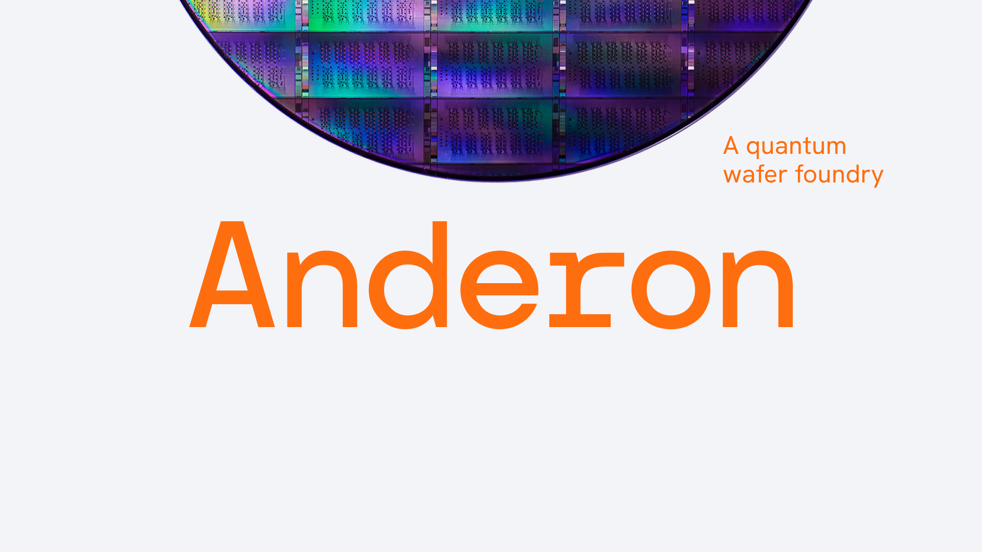
IBM has announced that it will create Anderon, a standalone company and America's first pure-play quantum chip foundry, backed by a proposed $1 billion CHIPS Act R&D award from the U.S. Department of Commerce and a matching $1 billion cash investment from IBM itself.
Headquartered in Albany, New York, Anderon will operate a 300mm quantum wafer fab and offer its manufacturing services to competing quantum hardware vendors. The deal was the centerpiece of a broader $2.013 billion federal quantum portfolio split across nine companies, the largest single quantum R&D commitment in U.S. history.
In launching Anderon, IBM is attempting to build the quantum computing industry's equivalent of TSMC, a neutral third-party manufacturer that’ll fabricate superconducting qubit wafers for other companies as well as IBM's own processors. No such foundry exists anywhere in the world today, with every operational quantum computer having been built by a vertically integrated company that designs, fabricates, and operates its own hardware.
A nine-company package
IBM's $1 billion award accounts for roughly half of the entire DoC quantum package. GlobalFoundries received a separate $375 million allocation to launch a "Quantum Technology Solutions" foundry covering multiple qubit architectures, including superconducting, trapped-ion, photonic, and silicon-spin designs. The remaining seven recipients each received smaller awards: D-Wave, Rigetti, Atom Computing, Infleqtion, PsiQuantum, and Quantinuum were each awarded $100 million, while Australian silicon-spin startup Diraq will receive up to $38 million.
Those seven non-foundry companies are required to give the federal government a minority, non-controlling equity stake in exchange for funding. Rigetti has also disclosed in a memorandum of understanding that the government will receive common stock at a 15% discount, while GlobalFoundries separately disclosed a 1% federal equity stake.
IBM's announcement contains no equivalent equity-stake disclosure for Anderon, a somewhat conspicuous omission given that the Trump administration converted part of Intel’s CHIPS Act manufacturing award into a roughly 10% government equity stake last year.
300mm wafer fabrication
IBM said back in November that all of its current and upcoming quantum processors are built on 300mm silicon wafers at the Albany NanoTech Complex, the largest public-private semiconductor R&D facility operated by the nonprofit NY CREATES. Jay Gambetta, IBM's Director of Research, wrote that the shift from 200mm to 300mm produces device output roughly 30 times faster by multiplying device complexity tenfold and tripling devices per line.
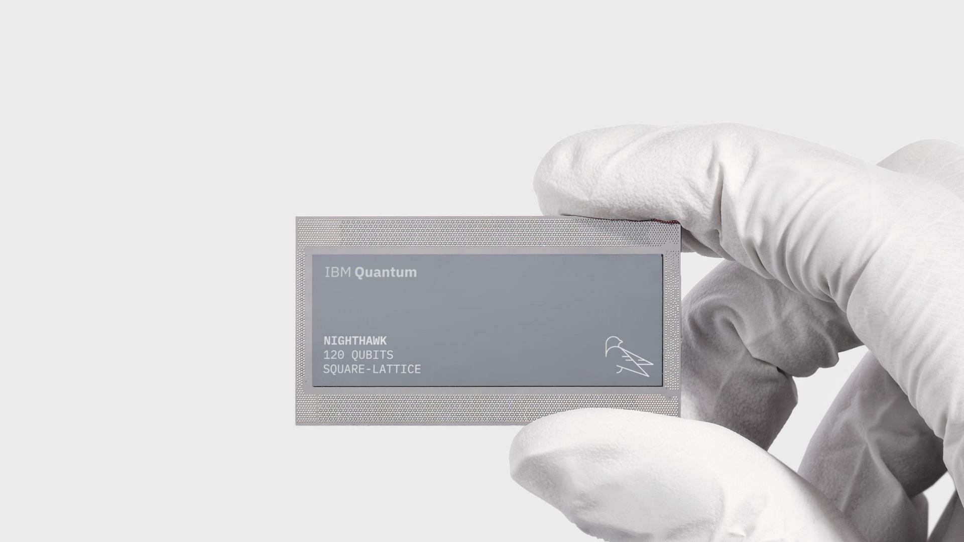
IBM's current production processor, Heron r2, holds 156 fixed-frequency qubits, while the Nighthawk processor, which went live via early access on IBM's quantum cloud in January, packs 120 qubits in a square lattice with 218 tunable couplers and a record median T1 coherence time of approximately 350 microseconds. IBM's fault-tolerance roadmap targets the Starling processor in 2029 at roughly 200 logical qubits running 100 million gates, followed by Blue Jay in 2033 at 2,000 logical qubits and 1 billion gates.
All of those chips need 300mm fabrication, and a dedicated foundry with established process design kits, in-line wafer testing, and baseline production routes could let other superconducting quantum companies skip the years and capital required to build their own cleanrooms. Anderon's initial process will support superconducting wiring, through-silicon vias, and bump interconnects, with plans to expand into other qubit modalities over time.
There’s an obvious comparison to TSMC here, which IBM is lapping up, but there’s also a fundamental difference: TSMC succeeded partly because its founder, Morris Chang, made an explicit promise not to compete with the companies that outsourced their fabrication. IBM obviously can’t credibly make that promise; it claims more than 90 operational quantum computers and an ecosystem spanning over 325 Fortune 500s, universities, and government agencies.
Quantum hardware startups considering Anderon will need to weigh 300mm production access against the risk of sharing process knowledge with their largest competitor. Google, which builds its own superconducting chips at its Santa Barbara facility and recently demonstrated quantum advantage on its 105-qubit Willow processor, is unlikely to outsource fabrication to IBM. IonQ and Quantinuum use trapped-ion architectures with almost no process commonality with superconducting silicon, and Microsoft's topological qubit program is on a different fabrication path entirely.
The near-term addressable market for Anderon is limited to other superconducting companies: Rigetti, IQM, SEEQC, and a handful of smaller companies, plus IBM itself. Whether any will actually outsource to a facility owned by their largest rival remains to be seen.
As for the choice of Albany, it carries some irony given that IBM's chip manufacturing presence in the region was effectively sold off in 2014 when the company paid GlobalFoundries $1.5 billion to take over its East Fishkill 300mm fab and Essex Junction 200mm fab. Those operations were losing roughly $700 million per year combined. GlobalFoundries later sold East Fishkill to ON Semiconductor in a deal finalized in 2023, and IBM and GlobalFoundries settled years of litigation over the original terms in January 2025.
The Albany NanoTech Complex, which sits on the SUNY Polytechnic campus, has received more than $25 billion in cumulative technology investment and hosts tenants including GlobalFoundries, Samsung, Applied Materials, ASML, Tokyo Electron, and Lam Research. In 2023, New York State committed $1 billion toward a High-NA EUV Accelerator at the complex as part of a broader $10 billion public-private partnership.
An escalating global spending race
The $2 billion U.S. quantum package comes amid a rapidly escalating global spending race. China's National Venture Guidance Fund, launched last March, authorized 1 trillion yuan, roughly $138 billion, across “hard technology” sectors, including quantum, with direct Chinese quantum investment estimated at $15 billion or more already deployed. Meanwhile, Japan has committed roughly $7.4 billion to semiconductors and quantum combined under its 2025 “Quantum Sun” industrialization agenda.
The EU Quantum Flagship is a rather paltry-by-comparison €1 billion, 10-year program. Combined with prior National Quantum Initiative spending and separate DARPA and Department of Energy programs, the CHIPS quantum package brings cumulative U.S. public quantum funding closer to parity with Europe and Japan but does little to close the gap with China.
BCG's widely cited estimate that quantum computing could generate up to $850 billion in economic value by 2040, which IBM referenced in its press release, is the optimistic end of a $450 to $850 billion range and describes end-user economic value, not vendor revenue. McKinsey's 2025 Quantum Technology Monitor projects a smaller $28 to $72 billion quantum computing revenue market by 2035, while Nvidia CEO Jensen Huang has publicly argued that practical quantum computing is 20 years away as a minimum.
It’s also worth noting that the Anderon deal isn’t yet finalized. CHIPS Act award histories show proposed amounts can shrink during due diligence: Samsung's manufacturing incentive, for example, fell from a proposed $6.4 billion in April 2024 to a finalized $4.75 billion by December 2024. Definitive documents between IBM and the DoC haven’t been executed.





 English (US) ·