
 2 hours ago
8
2 hours ago
8

Earlier this month, Samsung introduced the industry's first LPDDR5X-PIM memory, adding in-memory logic to the low-power memory standard, and at Hot Chips 2026, it dove into the memory technology that's we've previously seen at play through HBM stacks.
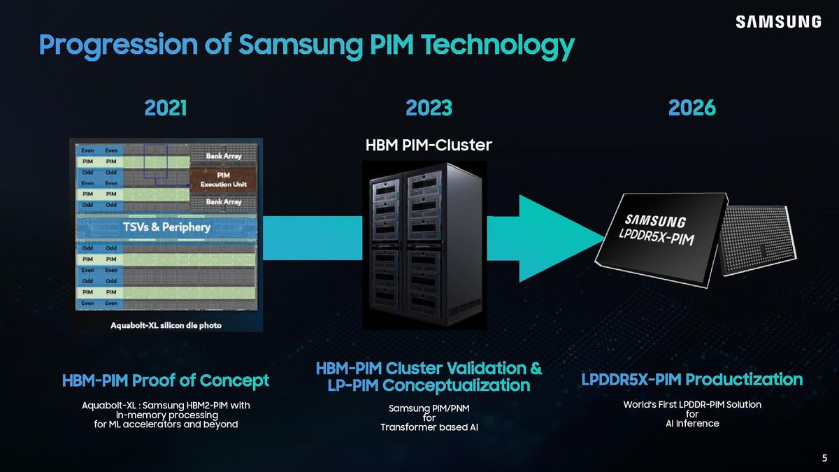
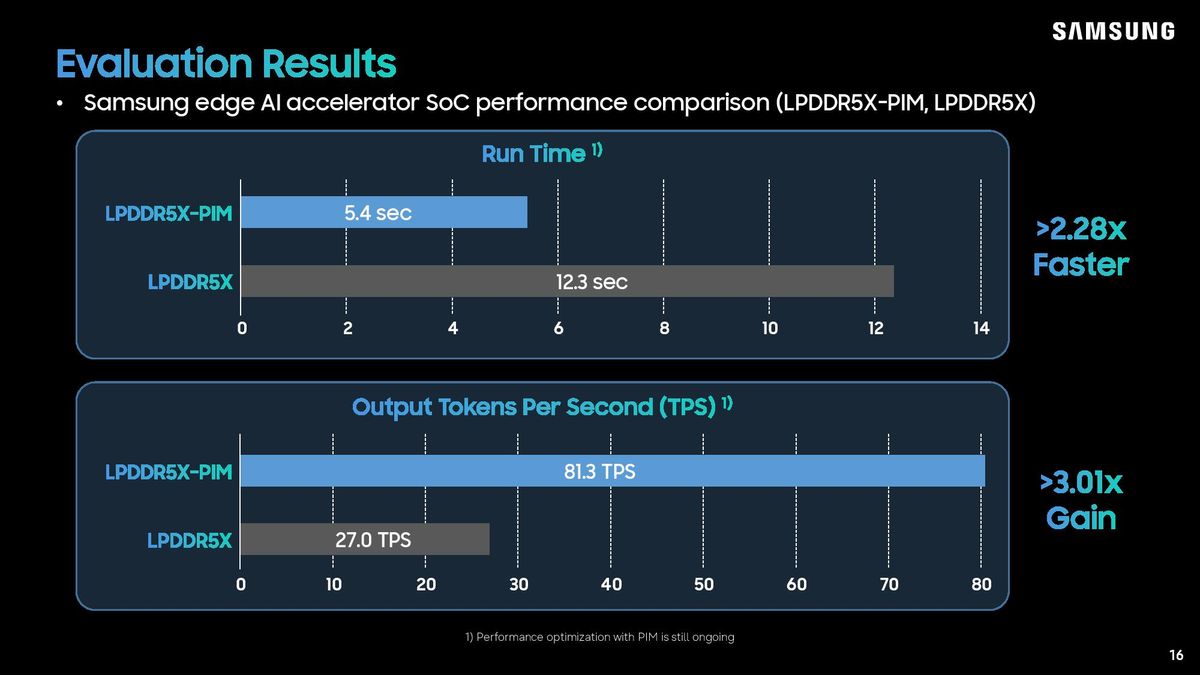
PIM, or Processing-in-Memory, is a technology Samsung demoed as early as 2021, piloted through HBM stacks in AMD accelerators. It's a small bit of logic that sits alongside DRAM cells, allowing basic calculations to happen directly in-memory. By handling those basic calculations locally, Samsung is able to eliminate the processor as a bottleneck and speed up, in particular, AI inference. In inference tasks, Samsung says its LPDDR5X-PIM is 2.28x faster than standard LPDDR5X, in fact.
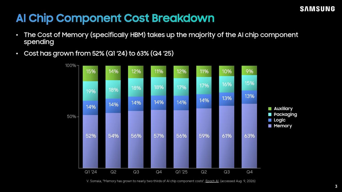
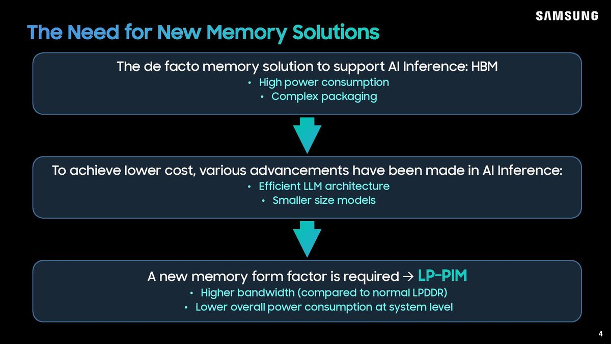
The reason for adding in-memory processing to LPDDR5X is pretty clear: HBM is too damn expensive. Micron warned just a day earning at Hot Chips that the HBM wafer demand is only getting worse, and Samsung opened its presentation with something we're all well aware of. Memory makes up the bulk of AI chip costs, and its share of the pie continues to grow. Add on top of that the power demands of DDR5, much less HBM, and LPDDR5X seems like an ideal target for PIM.
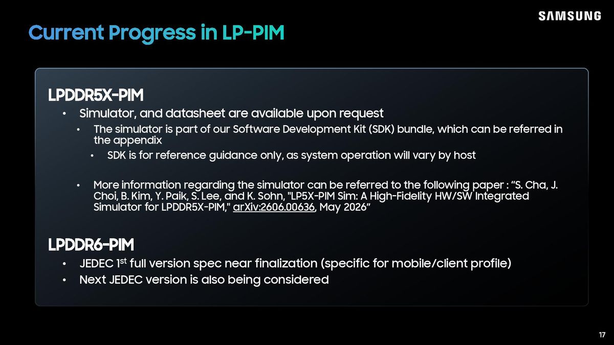
Samsung introduced HBM-PIM in 2023, and at the time, introduced the concept of LPDDR5X-PIM. What it shared at Hot Chips is a real product, taking the concept of LPDDR5X-PIM and putting it through validation. Samsung is also looking ahead for LPDDR6X-PIM, and the company says it hopes to have an initial specification from JEDEC this year.
Bringing in-memory processing to Samsung LPDDR5X
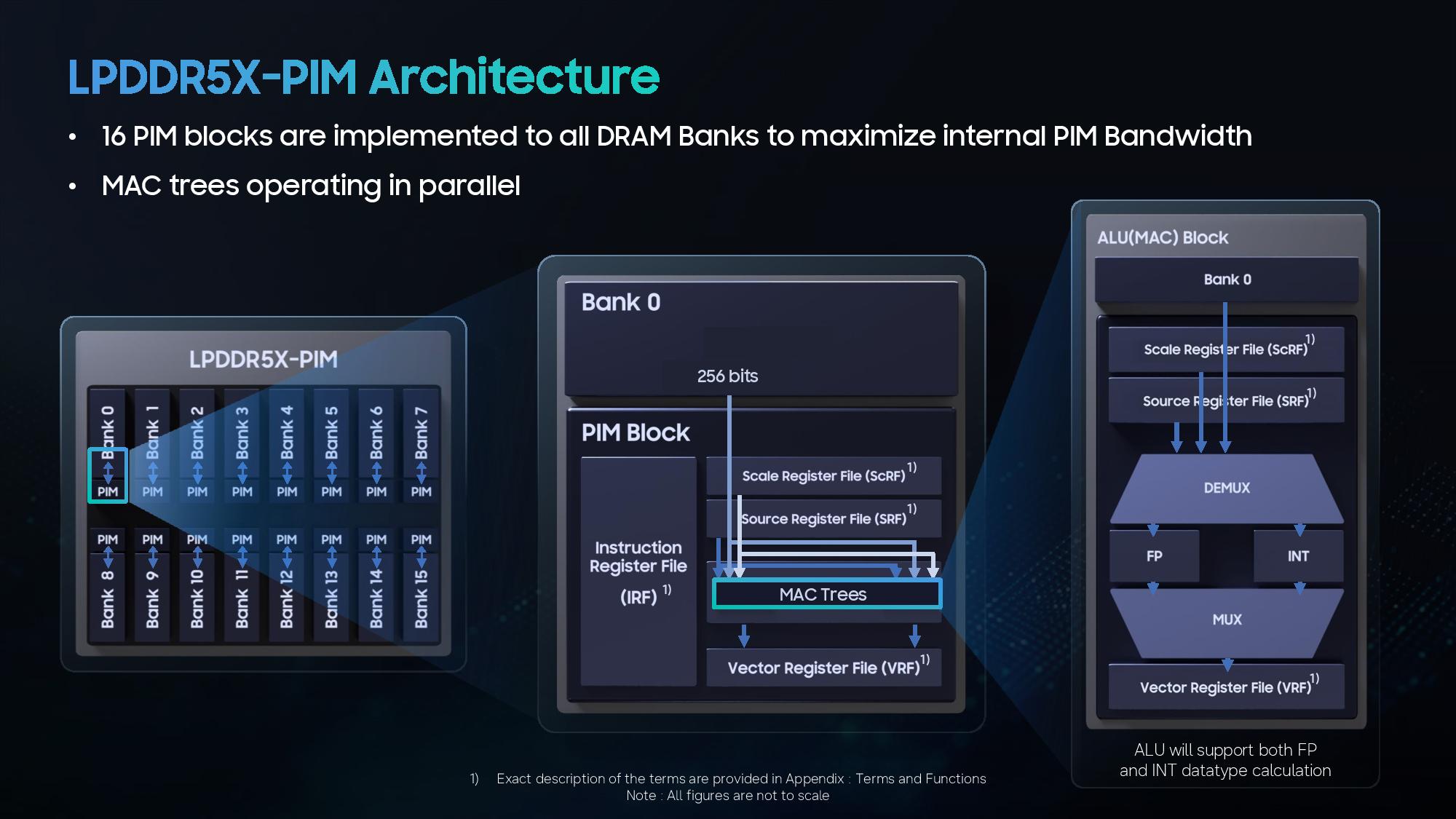
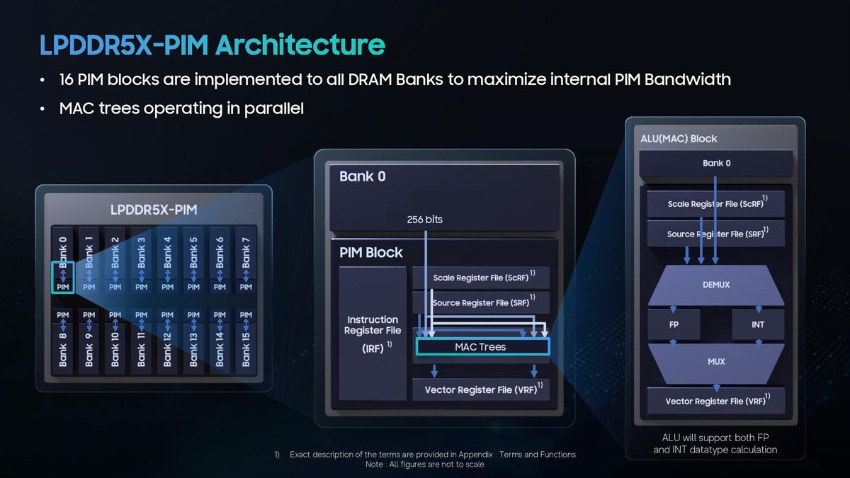
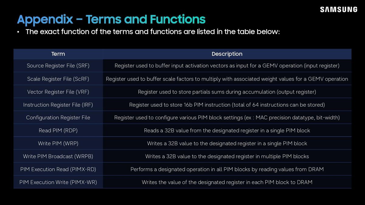
Above, you can see a basic layout of how Samsung integrated PIM into LPDDR5X. Each memory bank has its own PIM, which is an advancement over HBM-PIM, where Samsung had to cut banks to fit the logic. The memory bank, scale register file, and source register file feed parallel MAC trees. Once calculated, the output (either integer or floating point output) is written to a vector register file.
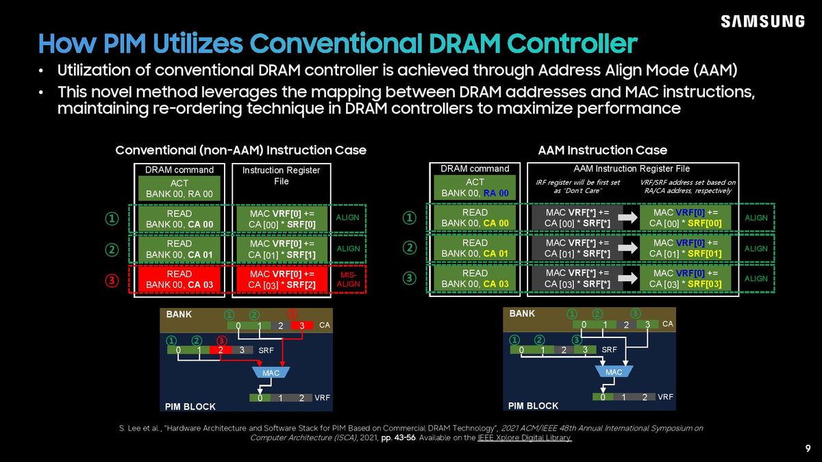
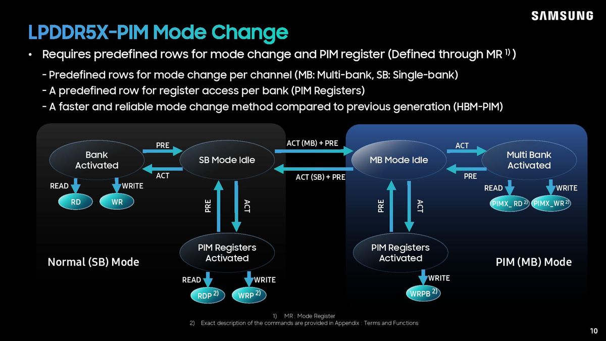
Samsung says its LPDDR5X can operate in two modes: single-bank (traditional DRAM) or multi-bank (PIM). Traditional DRAM controllers work, with commands switching between standard read/write or a PIM read/write depending on the mode. The challenge, according to Samsung, was reordering with conventional DRAM.
Samsung uses what it calls Address Align Mode (AAM) to get around the reordering issue. It maps DRAM addresses to MAC instructions, assigning the VRF/SRF address based on the RA/CA address, respectively, and not the Instruction Register File.
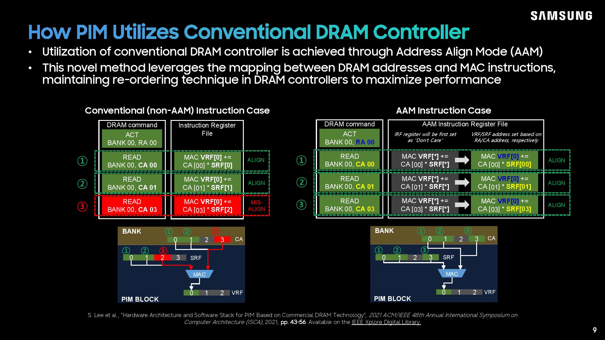
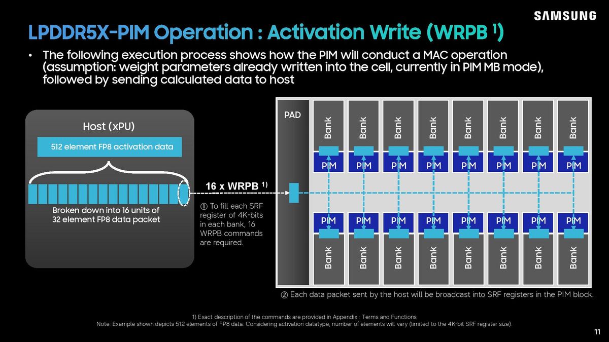
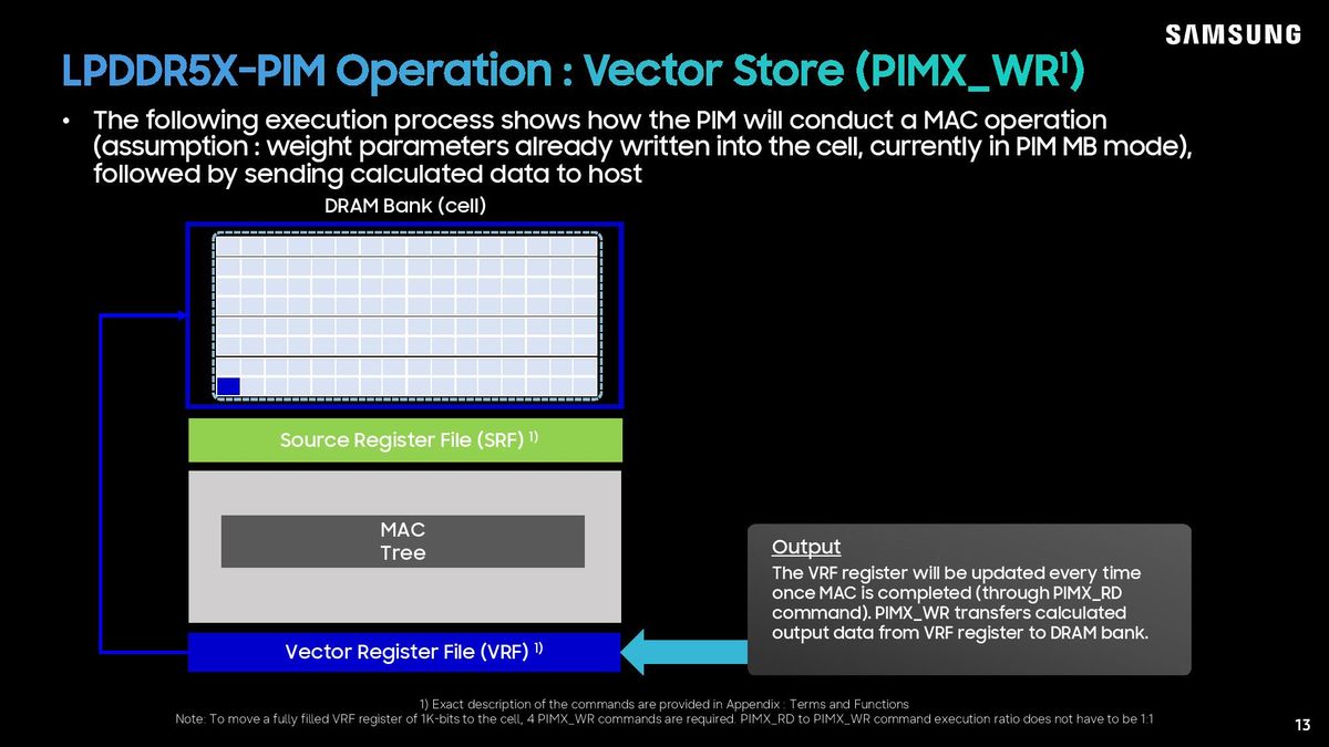
To demonstrate how data moves through the memory cells and calculations are performed, Samsung provided an example of a MAC operation, assuming weight parameters for the data are already written into the cell, and the memory is operating in multi-bank (PIM) mode.
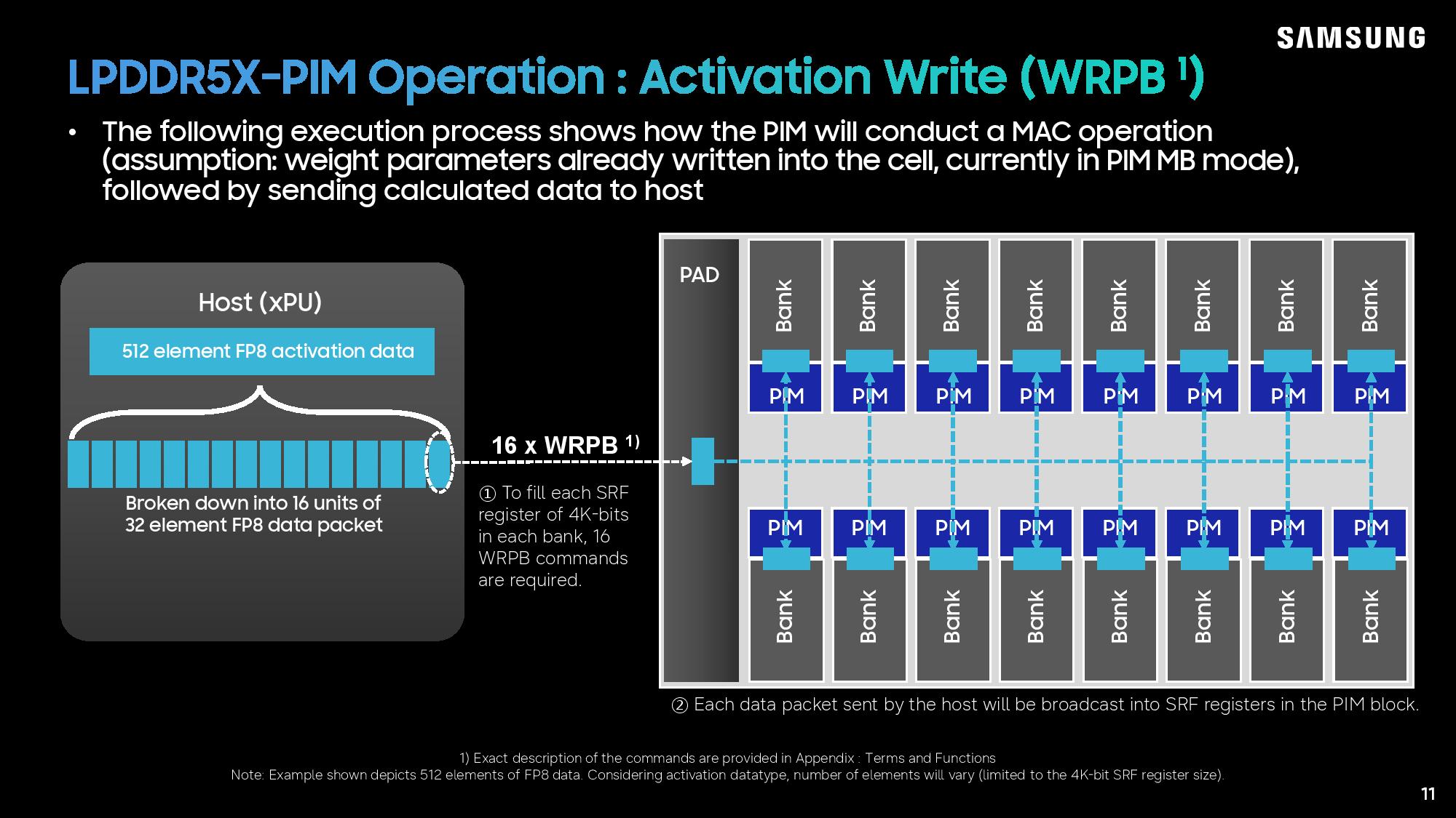
Storing 512 bytes of FP8 activation data, it's first broken down into 16, 256-bit packets, which are written into each of the banks in and noted in the Source Register File.
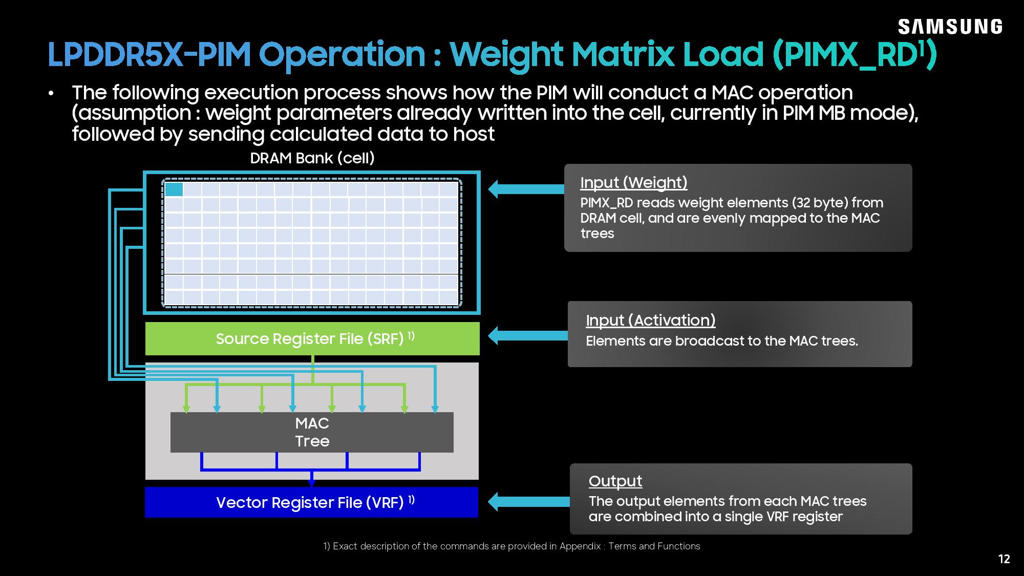
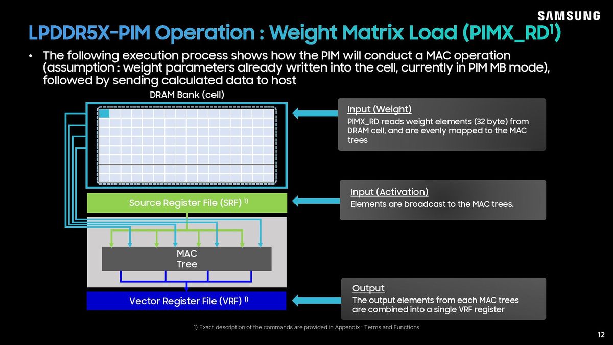
A PIMX_RD reads the weight data from the DRAM bank, feeding into the MAC trees alongside the data from the SRF. Once the calculation is done, the output vector from each operation is written into the Vector Register File.
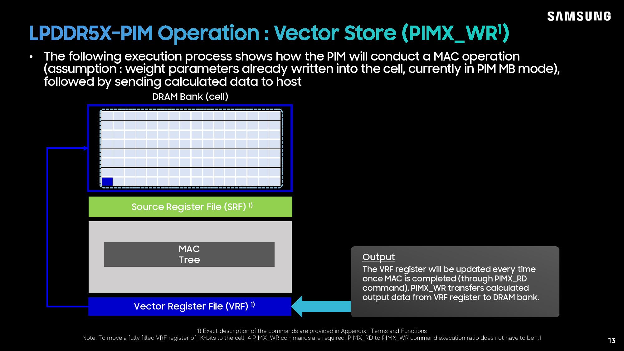
Once the calculation is done, a PIMX_WR command transfers the output data back to the DRAM bank. Samsung noted there doesn't need to be a 1:1 relationship between reads and writes, but it's useful for this example. With a VRF size of 1 kbit, a maximum of four calculations can be written to the VRF.
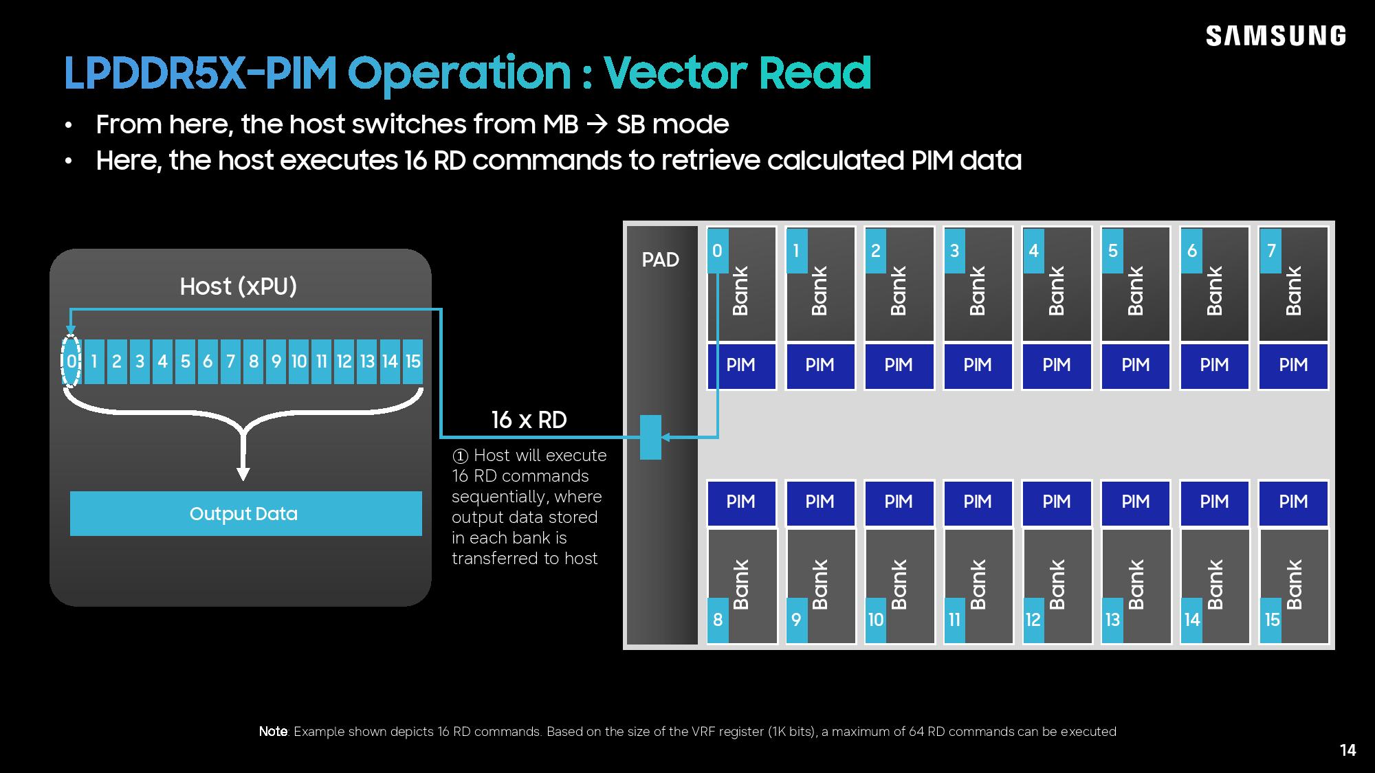
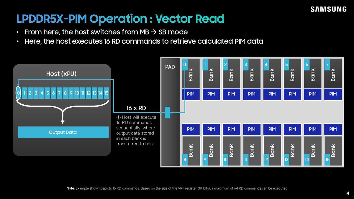
With the output written back to memory banks, the host just needs to read the data from memory. The host switches to single-bank (conventional DRAM) mode and executes 16 reads to gather the output from all of the memory banks.
Samsung LPDDR5X specs and preliminary performance
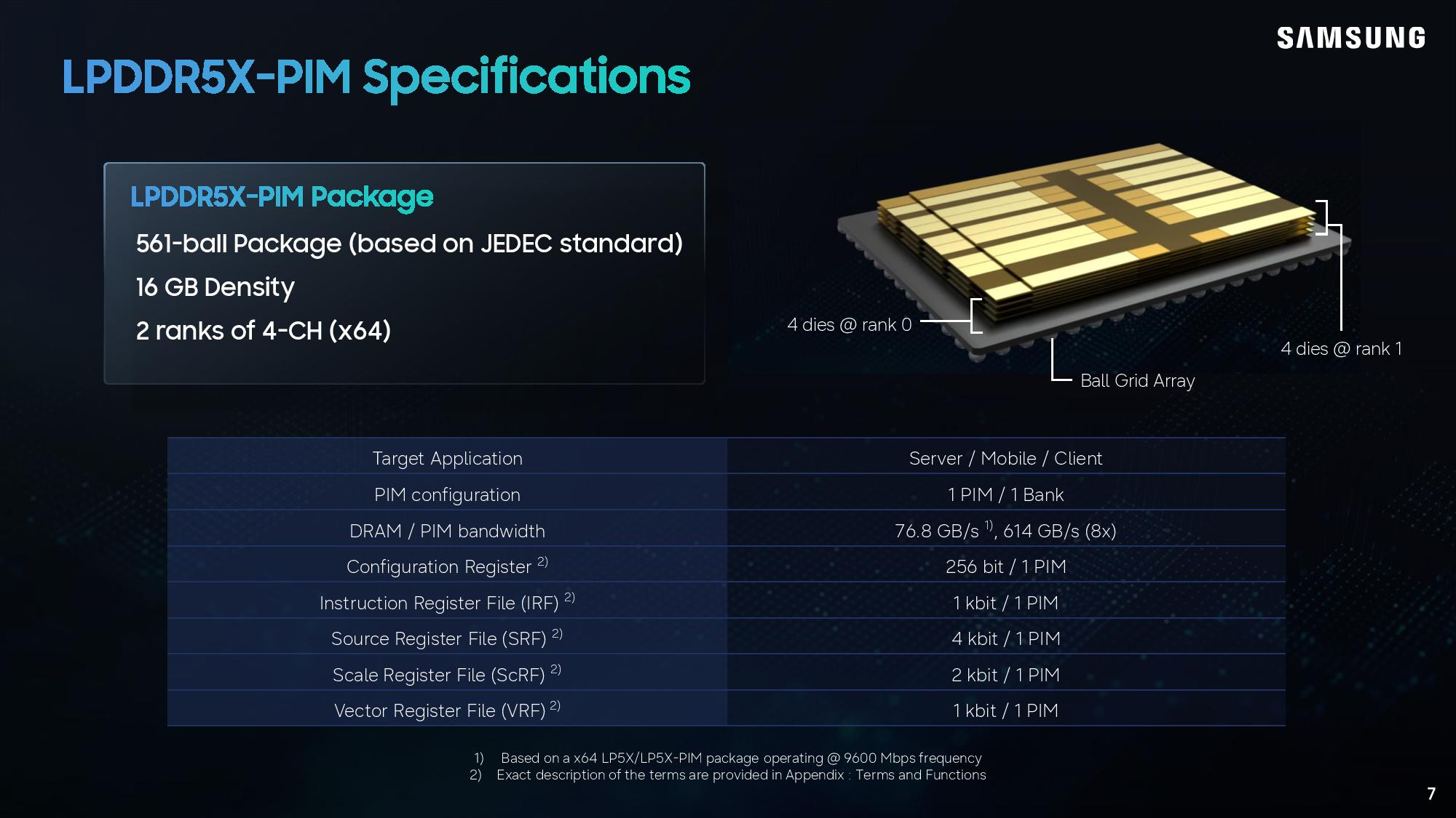
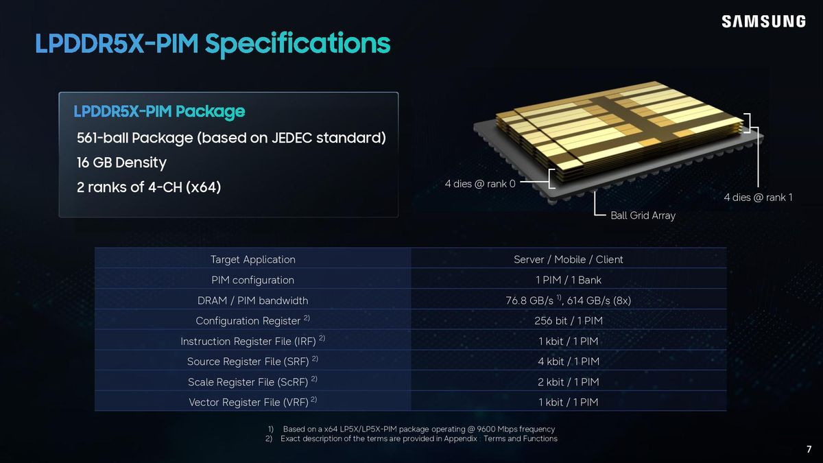
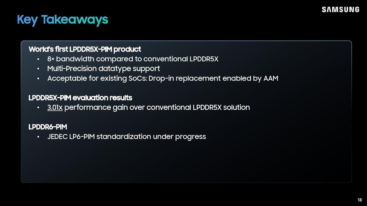
Samsung's LPDDR5X-PIM looks a lot like LPDDR5X. It uses a standard 561-ball array for packaging, just like LPDDR5X, and Samsung uses two 64-bit ranks with 16 GB modules. The critical number here is bandwidth. With LPDDR5X-9600, peak bandwidth is 76.8 GB/s, but that's increased by eightfold with PIM to 614 GB/s by reducing data movement and keeping basic logic local.
Samsung uses four dies per rank, for a total of eight dies. Not the various registers above, as well, as they're important for the illustration of data flow through Samsung's LPDDR5X-PIM memory.
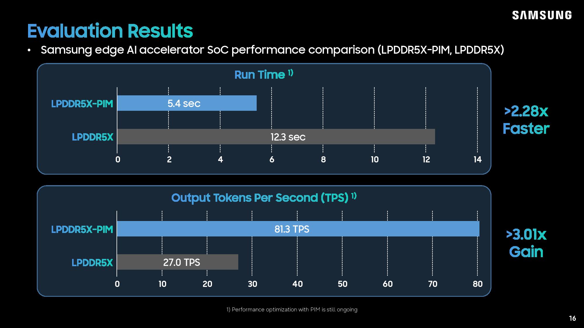
In Samsung's preliminary benchmarks, LPDDR5X-PIM is impressive. In model run time, Samsung say a 2.28x improvement with PIM, and in tokens per second (TPS), PIM offered a 3.01x increase in performance.
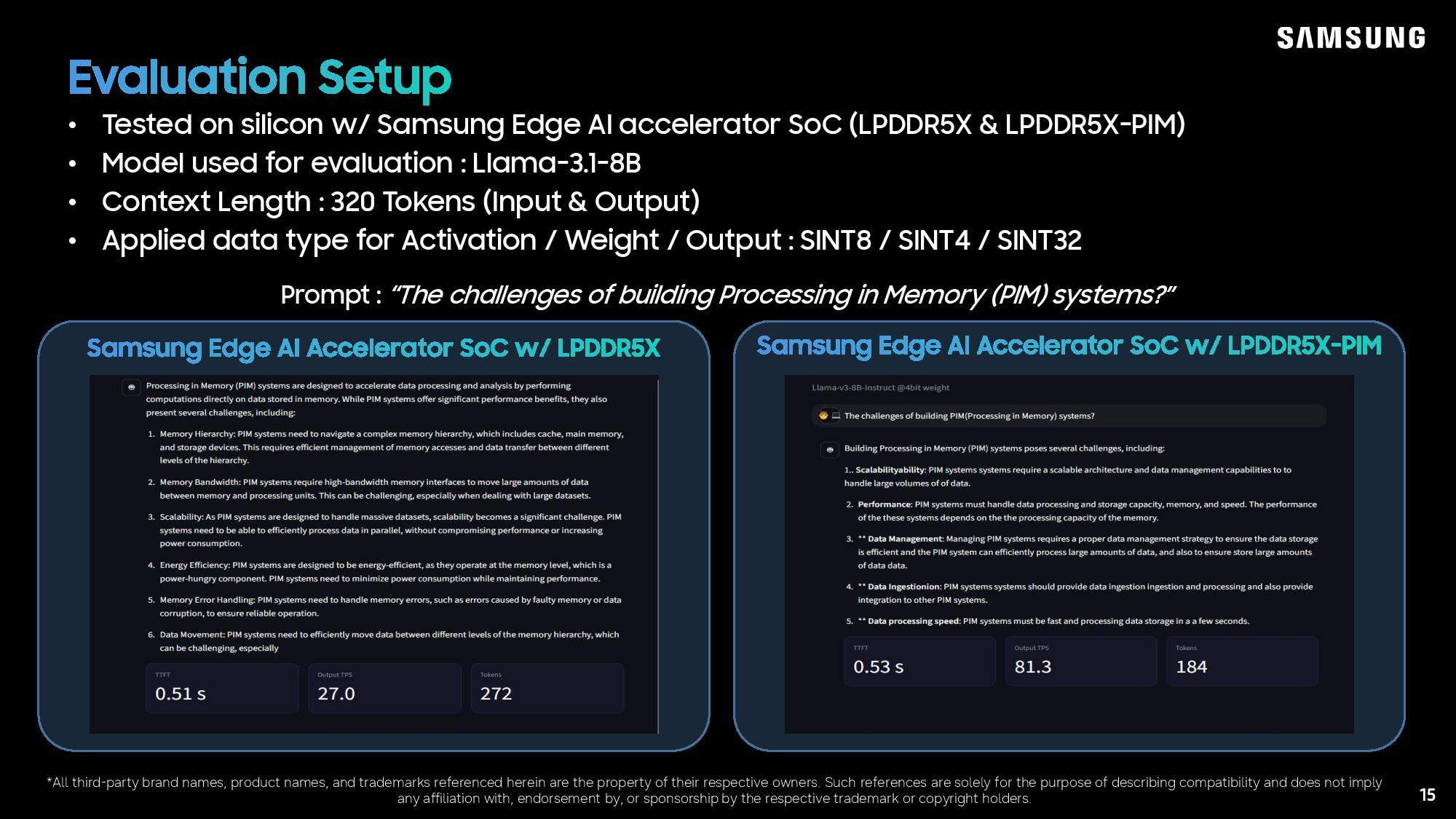
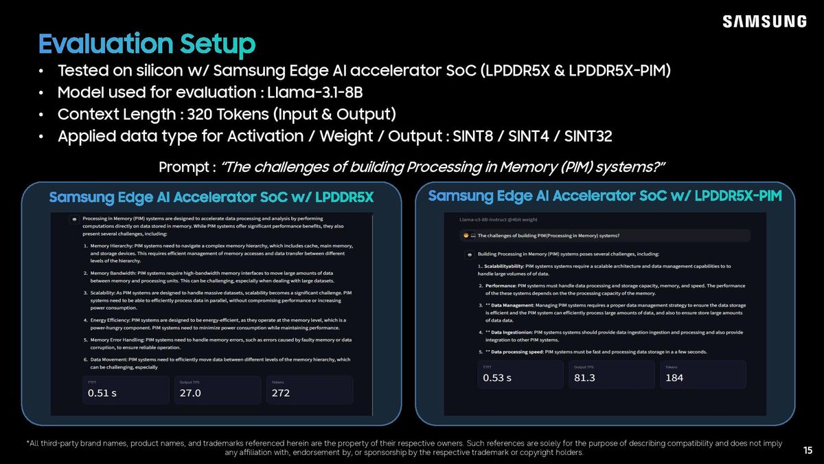
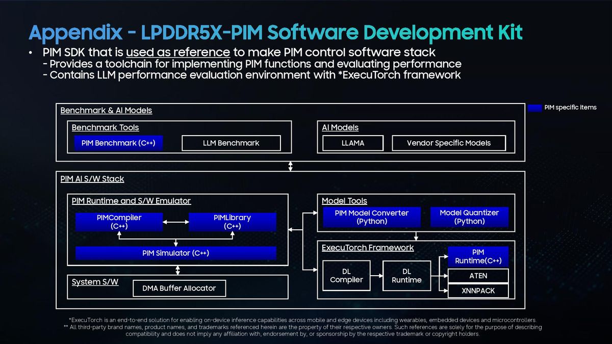
The slide above shows what happened behind the scenes to gather these numbers, with Samsung using an edge AI accelerator — we're not sure which, but perhaps an early Gaia SoC — and testing Llama 3.1 with 8 billion parameters. Notably, the output is different, which one attendee pressed Samsung about. The company says optimizations are ongoing to improve accuracy, but it expects the performance benefit to remain the same.
One of the main advantages of LPDDR5X is right there in the name: low power. With PIM, power consumption becomes more of a concern, but Samsung says it doesn't expect higher power consumption overall compared to conventional DRAM. The presenter noted that peak power consumption will be "much higher" due to the bursty power draw of the PIM, but Samsung still expects overall power draw to be lower than conventional DRAM.
That comes down to extra reads/writes. Although PIM represents a power increase, decreasing the number of times data needs to move between DRAM and the host will lead to overall lower power consumption. "We're not having significant power increase," as Samsung's Karam Hwang put it.
LPDDR5X has, until recently, only had applications in consumer products. However, SOCAMM2 serviceable modules allowed Nvidia to use LPDDR5X as the memory of choice with its Vera CPU. And Intel uses LPDDR5X with its new Crescent Island AI accelerator.
Even with PIM, LPDDR5X doesn't come remotely close to the bandwidth with available with HBM, but it has a lot of applications elsewhere. Samsung's targets of server, client, and mobile are telling, with LPDDR5X-PIM accelerating edge AI on mobile and client devices, as well as arriving in lower-scope accelerators like Crescent Island.
Full Samsung Hot Chips 2026 presentation
Image 1 of 19







 English (US) ·