
 10 hours ago
31
10 hours ago
31

At the ICC Global CEO Summit in Beijing, China Semiconductor Industry Association vice chairman Wei Shaojun claimed that a new domestically designed AI processor using mature 14nm logic and 18nm DRAM nodes can match the performance of Nvidia’s current 4nm chips. The architecture, which leverages 3D hybrid bonding and software-defined near-memory computing, is intended to counter China’s reliance on the Nvidia CUDA ecosystem.
Wei pitched the design as a potentially disruptive shift away from U.S. dependency, calling it central to China's AI strategy, but fell short of disclosing any specific technical details, hinting that he would “leave some suspense” for now, DigiTimes reports.
What he did describe was 14nm logic bonded directly to 18nm DRAM to drastically increase memory bandwidth and reduce compute latency. He said the system's power efficiency reaches 2 TFLOPS per watt, with a claimed total throughput of 120 TFLOPS, which is much higher than Nvidia’s A100 GPUs. He argued that by placing memory and logic in the same package, the chip avoids the “memory wall” that hinders large-scale GPU deployments.
Wei added that the chip is part of a fully domestic supply chain effort and will be formally disclosed in detail later this year. The ultimate goal, he said, is to sidestep Western supply chain constraints, cut costs, and decouple China’s AI development from U.S. vendors at both the hardware and software levels.
Memory wall and node stagnation
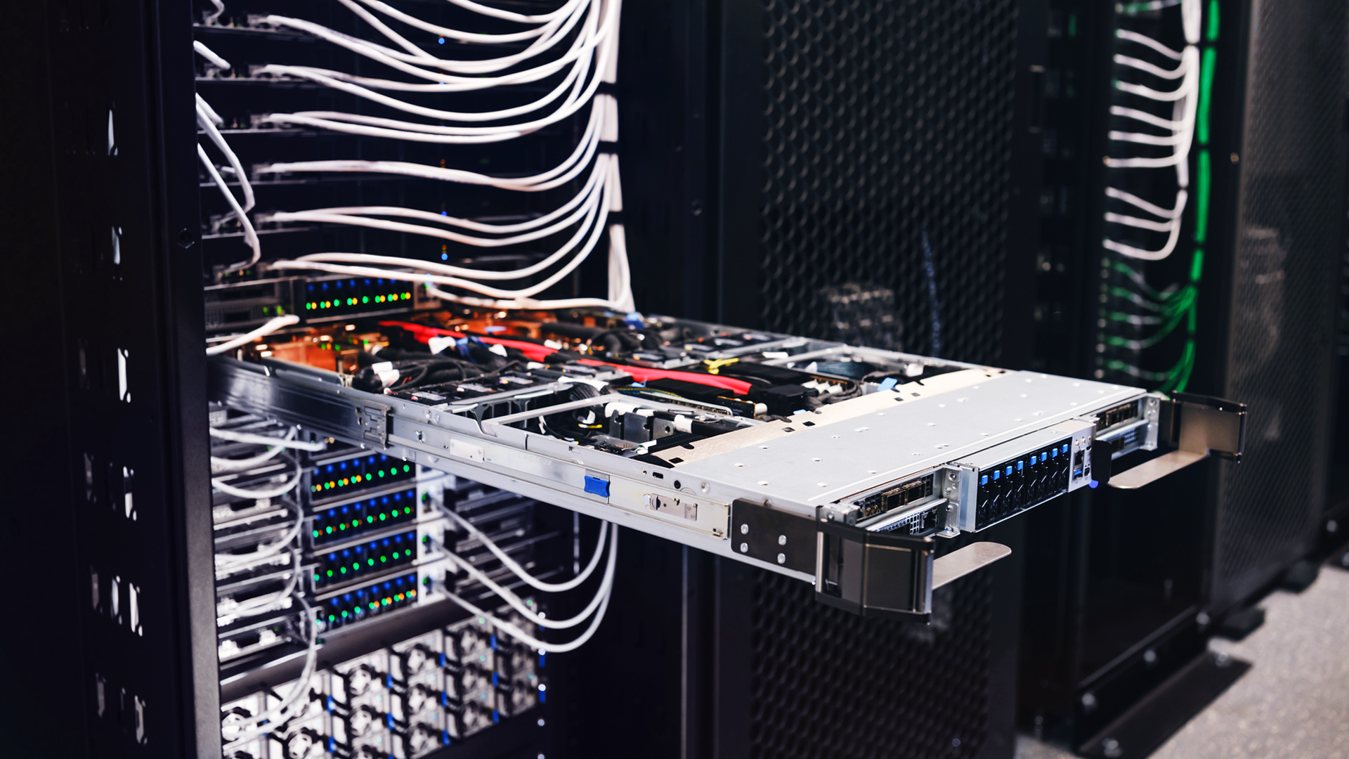
Wei's comments put forward a direct challenge to the dominant logic of semiconductor development over the last decade. Where U.S. and Taiwanese chipmakers have focused on smaller transistors — Apple's M3 at 3nm and Nvidia’s Hopper at 4nm — China’s researchers are now pitching advanced packaging and system architecture as a way to restore competitiveness using older manufacturing nodes.
The architecture described involves stacking a logic chip built on a 14nm process directly onto or alongside 18nm DRAM, using 3D hybrid bonding. This technique differs from traditional package-on-package or chiplet interconnects, in that it allows extremely dense, low-latency, high-bandwidth connections between dies. Unlike wire bonding or organic interposers, hybrid bonding directly fuses copper-to-copper contacts between wafers or die surfaces at the micron scale, supporting much higher interconnect density and thermal performance.
According to Wei, this layout enables near-memory compute, with logic operations executed in close proximity to memory blocks. That reduces the energy and latency cost of frequent memory fetches, often the limiting factor in AI workloads. He said software-defined logic further boosts efficiency by allowing compute units to be dynamically mapped and configured for AI-specific workloads.
He also suggested that a theoretical performance of 120 TFLOPS could be reached with a total power draw of 2 TFLOPS per watt, which would place the architecture well above the energy efficiency of Nvidia’s A100 and in the territory of Hopper-class or Blackwell-class chips. It also implies a significant advantage over CPU-bound systems like Intel Xeon, which Wei said remain less efficient for large model training.
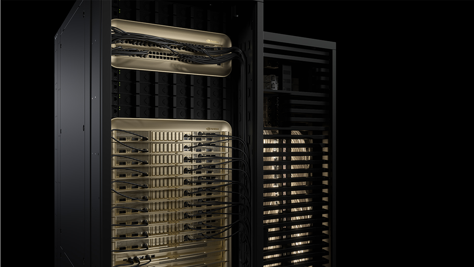
He stopped short of naming which Chinese firms are building silicon around this model, but past Chinese state media coverage has identified national champions such as Cambricon, Loongson, and Biren as players developing GPGPU-class accelerators. Cambricon in particular has previously discussed near-memory architectures and filed patents related to logic-in-memory compute.
CUDA dependency ‘traps’
Wei devoted a significant part of his address to outlining how he sees the entrenchment of CUDA as a vulnerability in the global AI industry. He argued that the early compatibility between large AI models and Nvidia’s GPGPU architecture created a cycle of increasing architectural dependency. Over time, software was designed for CUDA and Nvidia optimized its hardware for deep learning workloads, leading to what Wei called a "deep pit" of mutual dependence between model developers and GPU vendors.
He claimed that this dynamic leaves alternative architectures — such as domestic AI chips incompatible with CUDA — with almost no route to widespread adoption, regardless of theoretical performance. In his view, if China becomes similarly locked into this ecosystem, it will effectively lose sovereignty over its AI trajectory.
Wei is clearly not alone in this line of thought. Chinese companies such as Cambricon and Huawei have advanced CUDA alternatives and software abstraction layers in parallel with domestic AI hardware, with state-aligned investment efforts backing broader ecosystem development. Cambricon’s NeuWare stack, for instance, now offers compatibility with PyTorch, TensorFlow, and ONNX, and provides migration tools for CUDA-trained models. Alibaba and Huawei have similarly promoted their own developer frameworks targeting Ascend and XuanTie hardware.
Wei warned that continued reliance on U.S.-controlled software and toolchains would carry “very serious” consequences, both economically and geopolitically. He said China’s goal is to “abandon U.S. technology routes” and build a domestic AI technology stack that is resilient to supply chain shocks and regulatory constraints.
The Chinese are right to be concerned. In recent years, the U.S. has significantly expanded its export controls and blocked Nvidia from selling its leading hardware to Chinese firms. In response, the company introduced modified, lower-performance chips, which were also eventually restricted. Today, now that Nvidia has no market share left in China, domestic companies rely on legacy hardware or workarounds using second-tier accelerators and the grey market.
Not yet proven
The claims made at ICC raise questions that cannot yet be answered without detailed benchmarks and independent testing. While hybrid bonding is an established technology, the real-world performance of a full stack built on 14nm logic and 18nm DRAM remains to be seen.
Thermal dissipation in 3D stacks is still a major concern, particularly when logic and memory are in close proximity, and airflow is limited. Hybrid bonding also requires very high manufacturing precision and wafer alignment. These challenges could impact both yield and cost. China’s domestic foundries, including SMIC, are known to have strong 14nm-class production lines, but hybrid bonding at scale for logic-memory stacks would be a new capability.
Breaking Nvidia’s lock on the model training ecosystem also requires not just raw performance parity, but broad software support and capable developers. Even if China succeeds in building a functionally equivalent AI processor, adoption will remain limited without tooling and integration into PyTorch or TensorFlow workflows.
Still, with EUV lithography out of reach and GAA transistor designs still years away for domestic fabs, architectural innovation and packaging integration may be China’s most viable path to short-term competitiveness in high-performance AI workloads. Wei indicated that more technical details would be shared in future disclosures, but did not confirm whether working silicon had been produced.
Follow Tom's Hardware on Google News, or add us as a preferred source, to get our latest news, analysis, & reviews in your feeds.


 English (US) ·