
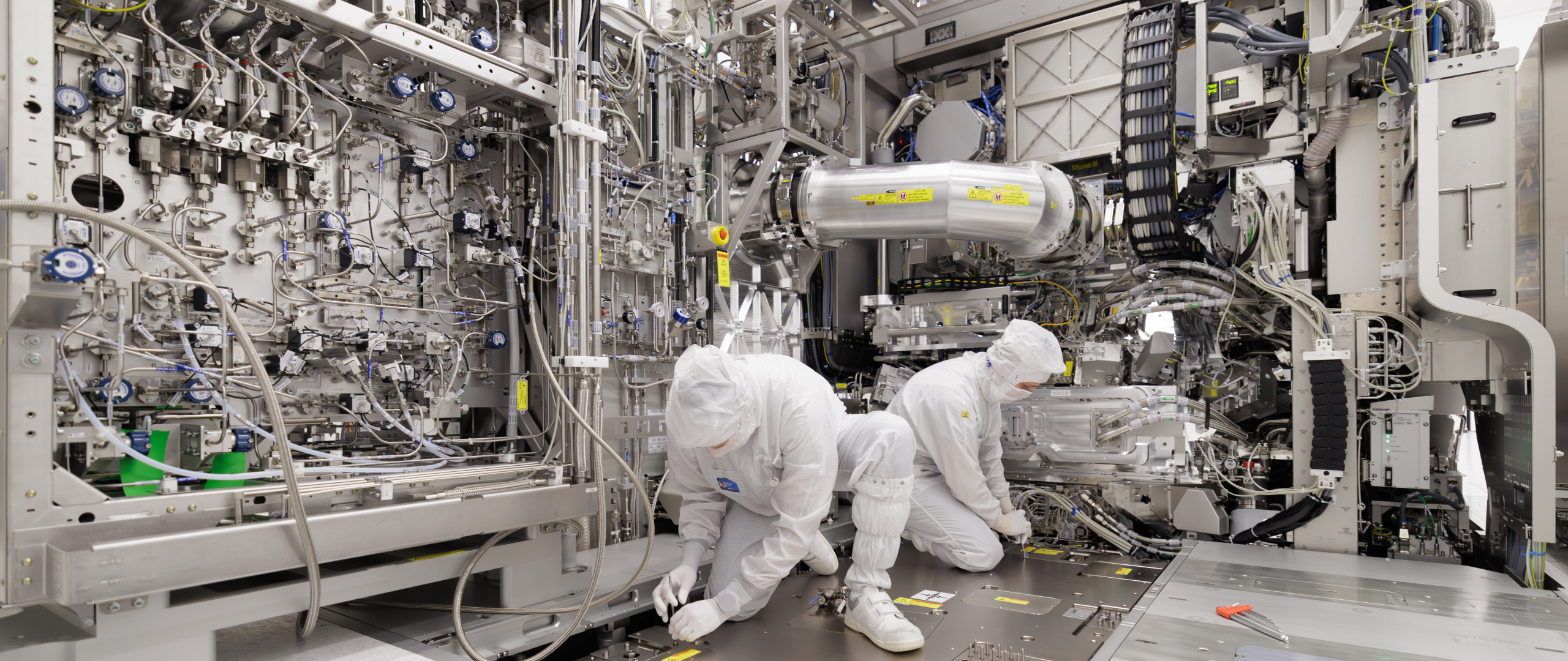
 8 hours ago
5
8 hours ago
5
ASML shipped 48 EUV lithography systems and 131 immersion DUV tools in 2025, generating €32.7 billion in total revenue and ending the year with a €38.8 billion order backlog.
The Dutch company holds a 100% monopoly on EUV lithography and approximately 83% of the global lithography market overall, and its roadmap now spans four distinct generations of technology: DUV immersion systems that still handle the majority of layers on every advanced chip, low-NA EUV scanners that enabled the 5nm and 3nm era, High-NA EUV tools now entering early production at Intel and Samsung, and a Hyper-NA concept that remains in feasibility studies for the 2030s.
Article continues below

DUV immersion and low-NA EUV
ASML's DUV immersion systems are still the backbone of semiconductor manufacturing when it comes to volume production, with the company selling 131 immersion DUV tools in 2025. Even a chip built on TSMC's 3nm node uses EUV on only a handful of critical layers; the majority of patterning steps still run on DUV immersion tools like the TWINSCAN NXT:2100i, which delivers 295 wafers per hour at 1.35 NA with 1.3nm overlay. DUV single-exposure is also the standard in mature nodes powering automotive and industrial chips. While DUV multi-patterning can push down to 7nm and even 5nm, it comes at an enormous cost of up to 34 patterning steps at 7nm versus nine with EUV.
Chinese customers purchased an estimated 70% of ASML's DUV immersion systems in 2024, stockpiling ahead of tightening Dutch export restrictions that now cover the NXT:1970i and newer models. SMIC demonstrated 7nm production using DUV multi-patterning for Huawei's Kirin 9000S, according to TechInsights. However, the process requires significantly longer cycle times than EUV-based production, and questions exist around whether yields are sufficient for volume commercialization.
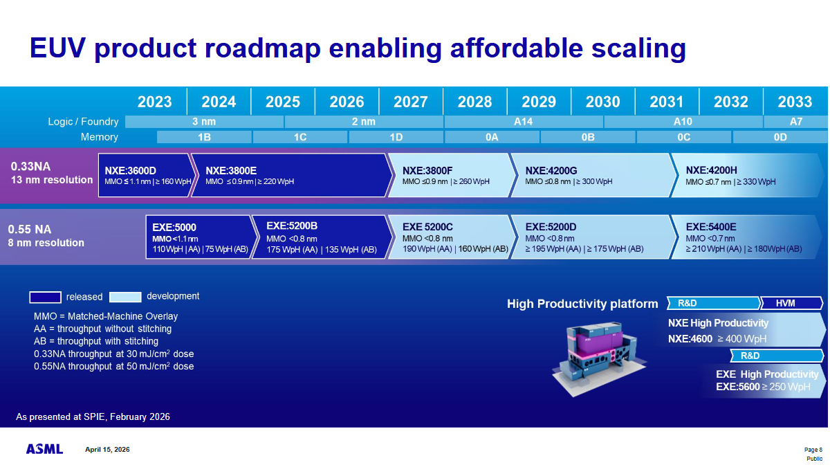
On the EUV side, ASML's low-NA systems operate at 0.33 numerical aperture with 13.5nm wavelength light, achieving 13nm single-exposure resolution. The TWINSCAN NXE:3600D, introduced around 2021, delivers 160 wafers per hour with 1.1nm matched-machine overlay. Its successor, the NXE:3800E, began shipping in March 2024 and pushes throughput to 195 wafers per hour, upgradable to 230 — following ASML's recently updated roadmap — while tightening overlay below 1.1nm. Each NXE:3800E costs roughly $180 million. It shares its bottom module, including wafer handler and faster stage mechanics, with the High-NA EXE platform, a decision that reduces ASML's manufacturing complexity and provides fabs with a degree of serviceability continuity when they upgrade.
ASML's roadmap extends low-NA further, with the NXE:3800F expected around 2027. It targets a ≤0.9nm overlay and over 260 wafers per hour. A subsequent NXE:4200G targets a ≤0.8nm overlay and over 300 wafers per hour, with an NXE:4200H beyond that at a ≤0.7nm and 330 wafers per hour. Further out, ASML has disclosed a High Productivity platform, the NXE:4600, targeting 400 wafers per hour or more.
Swipe to scroll horizontally
NA | System | Year | Logic node | Memory node | MMO | Throughput | Status |
0.33 | NXE:3600D | 2023 | 3nm | 1B | ≤1.1nm | ≥160 WpH | Released |
0.33 | NXE:3800E | 2024-2025 | 3nm/2nm | 1B/1C | ≤0.9nm | ≥220 WpH | Released |
0.33 | NXE:3800F | 2027-2028 | 2nm | 1D/0A | ≤0.9nm | ≥260 WpH | Development |
0.33 | NXE:4200G | 2030-2031 | A14 | 0B/0C | ≤0.8nm | ≥300 WpH | Development |
0.33 | NXE:4200H | 2032-2033 | A10/A7 | 0C/0D | ≤0.7nm | ≥330 WpH | Development |
0.33 | NXE:4600 | ~2031+ | High Productivity Platform | 0D | TBA | ≥400 WpH | R&D |
0.55 | EXE:5000 | 2023-2024 | 3nm | 1B | 110/75 WpH (AA/AB) | Released | |
0.55 | EXE:5200B | 2025-2026 | 2nm | 1C/1D | 175/135 WpH (AA/AB) | Released | |
0.55 | EXE:5200C | 2027-2028 | 2nm | 1D/0A | 190/160 WpH (AA/AB) | Development | |
0.55 | EXE:5200D | 2029-2030 | A14 | 0A/0B | ≥195/≥175 WpH (AA/AB) | Development | |
0.55 | EXE:5400E | 2032-2033 | A10/A7 | 0C/0D | ≥210/≥180 WpH (AA/AB) | Development | |
0.55 | EXE:5600 | ~2032+ | High Productivity Platform | Row 12 - Cell 4 | TBA | ≥250 WpH | R&D |
Meanwhile, TSMC has confirmed it will not use High-NA EUV for its A16 (1.6nm) or A14 (1.4nm) nodes, instead relying on low-NA with multi-patterning. Kevin Zhang, TSMC's Deputy Co-COO and Senior Vice President of Business Development, said at the company's European Technology Symposium last May that TSMC would adopt High-NA "whenever we see High-NA will provide meaningful, measurable benefit," adding that the technology team continues to extend the life of current EUV.
Computational lithography is one reason low-NA can stretch further, with ASML's Brion subsidiary developing inverse lithography technology and curvilinear mask optimization software that computationally corrects for optical distortion beyond specification, effectively squeezing better resolution from existing 0.33 NA optics without hardware changes.
TSMC has been a major user of these techniques, and their continued advancement narrows the gap between low-NA double patterning and High-NA single exposure. ASML's installed base management business, which services and upgrades the global fleet of lithography tools, reached €8.2 billion in revenue in 2025, up 26% year-over-year. That recurring revenue stream grows with every tool shipped and is increasingly important as fabs push older systems to higher utilization rates.
High-NA EUV
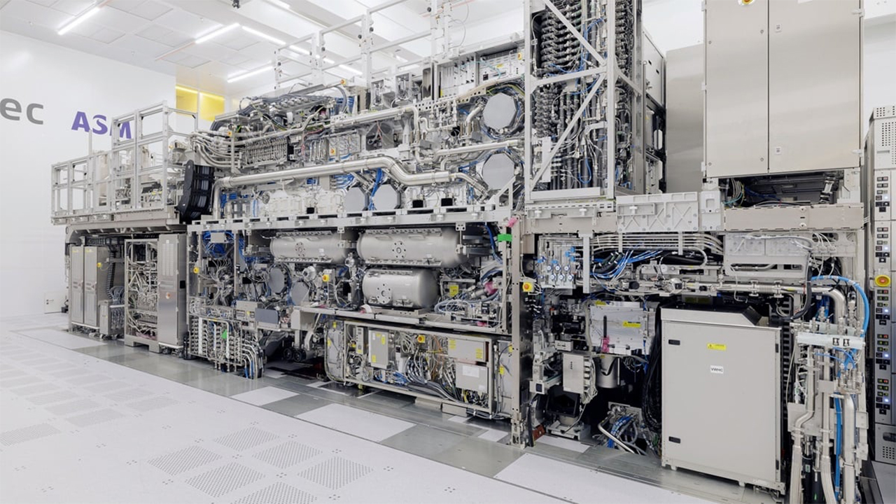
The jump to 0.55 numerical aperture with high-NA is the largest optical leap in EUV's history, shrinking minimum resolution from 13nm, which itself was down from 30nm with DUV, to 8nm and enabling approximately 2.9 times higher transistor density in a single exposure. ASML's first High-NA tool, the EXE:5000, shipped to Intel in December 2023 as a development platform.
Each unit of the production-capable EXE:5200B weighs in at 150,000 kilograms, requires 250 shipping crates, and takes six months and 250 engineers to assemble on-site, says Intel. Priced at approximately $380 million, the EXE:5200B delivers 175 wafers per hour at 50 mJ/cm² dose with 0.7nm overlay. ASML told Reuters in early 2024 that it had taken 10 to 20 orders by that point and planned to deliver 20 annually by 2028.
Intel announced that it had completed acceptance testing of its EXE:5200B in December 2025 at its Hillsboro D1X fab and that the tool will be used for the development of Intel's 14A fabrication process. 14A is expected to be the first production node to rely on High-NA for its most critical layers, with risk production targeted for 2027.
In September, SK hynix became the first memory manufacturer to install a commercial High-NA system at its M16 fab in Icheon, South Korea. Samsung, meanwhile, received its first EXE:5200B in October, with a second unit due in the first half of 2026 for its 1.4nm foundry node. Imec, the Belgian research institute, secured an EXE:5200 last month with a Q4 2026 qualification target for sub-2nm process development.
ASML's near-term High-NA roadmap includes the EXE:5200C, targeting 190 wafers per hour without stitching and 160 with stitching at sub-0.8nm overlay, followed by the EXE:5200D at 195/175 wafers per hour and eventually the EXE:5400E at 210/180 wafers per hour with sub-0.7nm overlay. A High Productivity variant, the EXE:5600, targets 250 wafers per hour or more.
Analysts from SemiAnalysis believe TSMC won’t adopt High-NA EUV until its 1nm-class A10 node, which would place volume deployment around 2029 to 2030, because existing low-NA EUV systems can match High-NA's 8nm resolution using double patterning, and SemiAnalysis estimates that approach may still cost less than High-NA single patterning. High-NA tools also require substantial changes to existing fab buildings to accommodate their size.
Hyper-NA and pellicles
ASML placed Hyper-NA on its official roadmap for the first time at imec's ITF World in May 2024, with former CTO Martin van den Brink commenting a few months prior that an NA above 0.7 "is certainly an opportunity that will become more visible from around 2030." The primary target is 0.75 NA, with 0.85 NA also under investigation. Zeiss has begun preliminary lens designs. Estimated tool cost: roughly $720 million per system, according to TrendForce.
At 0.75 NA, however, polarization effects begin destroying imaging contrast because one polarization orientation effectively cancels light at extreme incidence angles, thereby necessitating the use of polarizers that block photons and reduce efficiency. Depth of focus shrinks further, and resists must be made even thinner than the sub-30nm films used for high-NA, worsening etch selectivity and stochastic defects from photon shot noise. On top of all that, an electron blur of approximately 2nm may impose a solid resolution barrier regardless of optical improvements.
Pellicle development is another bottleneck. These ultra-thin membranes protect masks from particle contamination during exposure but must transmit EUV light efficiently at rising source power levels. ASML's current composite silicon-based pellicle achieves over 90% transmission at 380 W source power, but for future systems running at 600 W to 1,000 W, carbon nanotube pellicles are the next-gen technology, achieving up to 97% transmission while withstanding temperatures above 1,500 C. Mitsui Chemicals is building dedicated CNT pellicle production capacity targeting 5,000 sheets per year and commercialization aimed for this year.
Export controls and Canon NIL
EUV systems have never been sold to China, blocked since 2019 under U.S. pressure despite existing orders from Chinese customers. In addition, Dutch export controls, effective since late 2023, required licenses for advanced DUV immersion systems (NXT:2000i and newer), and by September 2024, the restrictions expanded to include the NXT:1970i and NXT:1980i.
Servicing restrictions also prohibit ASML from improving overlay accuracy or increasing throughput by more than 1% on installed Chinese systems. China represented 49% of ASML's revenue at the peak of stockpiling in Q2 2024, falling to roughly 36% for full-year 2024. ASML's management guided China to approximately 20% of revenue in 2025 and 2026, which has seen South Korea and Taiwan emerge as the primary growth markets, with SK hynix alone placing a record $7.9 billion EUV order last month covering roughly 30 systems over two years.
Canon's FPA-1200NZ2C nanoimprint lithography system, announced in October 2023, represents the only credible alternative patterning approach. At roughly $15 to $20 million per system with 90% lower power consumption than EUV, it uses direct mechanical pattern transfer rather than optical exposure. Canon delivered the first commercial unit to the Texas Institute for Electronics in September 2024, and its current specs show some significant limitations: 80 to 100 wafers per hour (versus 195+ for low-NA EUV), 14nm minimum linewidth, and 2.4 to 3.2nm overlay (versus sub-1.1nm for EUV).
Japan's Dai Nippon Printing (DNP) is targeting 2027 mass production of 1.4nm-class nanoimprint templates, but no major foundry has committed to NIL for high-volume logic manufacturing. The technology's likely niche remains repetitive memory patterns, particularly high-layer-count 3D NAND, where its cost advantage could outweigh the throughput and overlay penalties. Defect density from direct physical contact between template and resist remains the fundamental barrier to logic adoption, where a single misplaced particle can kill an entire die.
ASML revenues continue climbing
ASML's 2025 results reflect the sheer scale of its roadmap, with €32.7 billion in revenue (up 16% year-over-year), 52.8% gross margin, and €9.6 billion net income. EUV became the leading source of system revenue at 48%, or €11.6 billion, up 39% from 2024. Net bookings surged 48% to €28 billion, with Q4 2025 alone delivering a record €13.2 billion in orders. The company recognized revenue on two High-NA systems during the year.
ASML's Q1 2026 results, published April 15, show €8.8 billion in total net sales at 53% gross margin, with €2.8 billion net income. The company shipped 16 EUV and 17 immersion DUV systems in the quarter, with South Korea accounting for 45% of system sales by region and China at 19%. ASML raised its full-year 2026 revenue guidance to €36 to €40 billion, with 51% to 53% gross margins
Each NA increase delivers diminishing resolution gains at exponentially rising cost and complexity. The most likely trajectory is not a clean generational handoff but an extended coexistence: low-NA handling the bulk of EUV layers well into the 2030s, High-NA reserved for the most critical pitches at sub-2nm nodes, and Hyper-NA arriving as a targeted tool for the most extreme features, subject to workarounds for the bottlenecks we’ve discussed above.


 English (US) ·