
 1 month ago
44
1 month ago
44
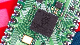
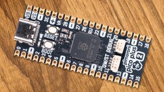
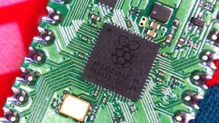
The new Raspberry Pi Pico 2, released just two weeks ago, has garnered a lot of attention from the maker community. Powered by the RP2350, the Pico 2 comes with two different CPUs in one package. The first is a powerful dual-core Arm Cortex M33, the second is RISC-V based and designed as a personal project by Raspberry Pi engineer Luke Wren.
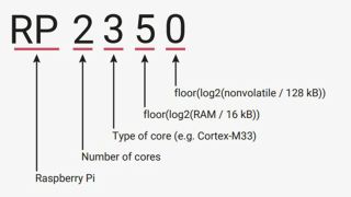
The RP2350 gets its name as follows:
- RP
- Raspberry Pi
- 2
- Number of cores
- 3
- Type of core (Cortex M33)
- 5
- SRAM Memory capacity (520KB)
- 0
- Internal storage capacity (0 for RP2350A and B, 4 for 2MB onboard found in the RP2354A and B)
RP2350 Block Diagram
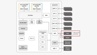
The RP2350’s Arm Cortex M33 cores are more powerful than the Arm Cortex M0+ found on the original RP2040 of the Raspberry Pi Pico and the Raspberry Pi Pico W, But the most intriguing feature has to be the dual core RISC-V Hazard3 CPU. This CPU has performance somewhere between the Arm Cortex M0+ of the RP2040 and the Arm Cortex M33 of the RP2350. It is the first Raspberry Pi product to use RISC-V architecture, but it may not be the last. Just don’t go expecting to see it pop up in the successor to the Raspberry Pi 5.
The release of the Raspberry Pi Pico 2 saw the $5 upgrade to the original, and dare we say beloved original Pico. For only an extra dollar we get lots more performance, nut, the RP2350 isn’t the only chip to be released. The RP235X are a series of chips based on the same CPU and RAM configuration, but some have onboard storage and an even greater number of GPIO pins.
RP235X Packages
Swipe to scroll horizontally
| RP2350A | QFN-60 | 7mm^ | None | 30 | 4 | $1.10 | $0.80 |
| RP2350B | QFN-80 | 10mm^ | None | 48 | 8 | $1.20 | $0.90 |
| RP2354A | QFN-60 | 7mm^ | 2MB | 30 | 4 | $1.30 | $1 |
| RP2354B | QFN-80 | 10mm^ | 2MB | 48 | 8 | $1.50 | $1.10 |
The RP2350A, as used in the Raspberry Pi Pico 2 has the following specifications.
Swipe to scroll horizontally
| SoC | RP2350, Dual Core Arm Cortex M33 or Dual Core RISC-V Hazard3 running at up to 150 Mhz |
| SRAM | 520 KB |
| Flash Storage | 4MB QSPI |
| Security | Arm TrustZone, 8KB OTP, Secure Boot |
| Wi-Fi / Bluetooth | None |
| Language Support | MicroPython, CircuitPython, C, C++ |
| USB Interface | USB 1.1 Device and Host |
| GPIO Logic Level | 3.3V |
| GPIO | 26 x Digital IO |
| 4 x 12-bit ADC (Analog pins) | |
| 2 x UART, 2 x I2C, 2 x SPI, 24 x PWM | |
| Programmable IO | 12 PIO State Machines |
| Onboard LED | GPIO 25 |
| Power | 1.8 to 5.5V via Micro USB or VSYS |
| MCU Sleep Mode | <10uA |
| Dimensions | 21 x 51mm |
| Price | $5 |
If we compare the RP2350A package with the specifications of the Pico 2 we note that the RP2350A (and RP2350B) has no internal storage. Instead the RP2350A and B use external QSPI storage, just like the original Raspberry Pi Pico’s RP2040. But the RP2354A and B offer 2MB of on-chip stacked storage via a Winbond W25Q16JVW connected to the QSPI interface.
We’ve seen plenty of RP2350A and B powered boards, but nothing has emerged about the RP2354 chip, nor any products which are powered by it.
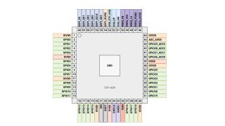
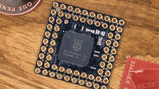
The RP2350A and the RP2354A are both 7mm^ QFN-60 packages with 30 GPIO pins broken out around the 7mm^ square chip. The GPIO provides UART, SPI, I2C, 24 PWM and four analog to digital converters, used for analog input. These analog pins are mapped to physical pins 40 to 43 (GPIO 26,27,28 and 29) on the top right of the chip.
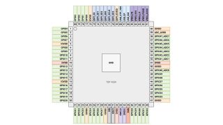
The RP2350B and the RP2354B are both 10mm^ QFN-80 packages and the extra area affords the chip more GPIO pins. Boosted from the 30 GPIO pins found in the RP2350A and RP2354A, the RP2350B and RP2354B have 48 GPIO pins. But what are the extra pins? We’ve mapped them out to compare the physical pin references between the QFN60 and QFN80 packages.
Swipe to scroll horizontally
| 1 | IOVDD Power supply for digital GPIOs, nominal voltage 1.8 V to 3.3 V | GPIO4 |
| 2 | GPIO 0 | GPIO5 |
| 3 | GPIO1 | GPIO6 |
| 4 | GPIO2 | GPIO7 |
| 5 | GPIO3 | IOVDD Power supply for digital GPIOs, nominal voltage 1.8 V to 3.3 V |
| 6 | DVDD Digital core power supply, nominal voltage 1.1 V | GPIO8 |
| 7 | GPIO4 | GPIO9 |
| 8 | GPIO5 | GPIO10 |
| 9 | GPIO6 | GPIO11 |
| 10 | GPIO7 | DVDD Digital core power supply, nominal voltage 1.1 V |
| 11 | IOVDD Power supply for digital GPIOs, nominal voltage 1.8 V to 3.3 V | GPIO12 |
| 12 | GPIO8 | GPIO13 |
| 13 | GPIO9 | GPIO14 |
| 14 | GPIO10 | GPIO15 |
| 15 | GPIO11 | IOVDD Power supply for digital GPIOs, nominal voltage 1.8 V to 3.3 V |
| 16 | GPIO12 | GPIO16 |
| 17 | GPIO13 | GPIO17 |
| 18 | GPIO14 | GPIO18 |
| 19 | GPIO15 | GPIO19 |
| 20 | IOVDD Power supply for digital GPIOs, nominal voltage 1.8 V to 3.3 V | GPIO20 |
| 21 | XIN Connect a crystal to RP2350’s crystal oscillator | GPIO21 |
| 22 | XOUT Connect a crystal to RP2350’s crystal oscillator | GPIO22 |
| 23 | DVDD Digital core power supply, nominal voltage 1.1 V | GPIO23 |
| 24 | SWCLK Access to the internal Serial Wire Debug multi-drop bus; provides debug access to both processors | IOVDD Power supply for digital GPIOs, nominal voltage 1.8 V to 3.3 V |
| 25 | SWDIO Access to the internal Serial Wire Debug multi-drop bus; provides debug access to both processors | GPIO24 |
| 26 | RUN Global asynchronous reset pin | GPIO25 |
| 27 | GPIO16 | GPIO26 |
| 28 | GPIO17 | GPIO27 |
| 29 | GPIO18 | IOVDD Power supply for digital GPIOs, nominal voltage 1.8 V to 3.3 V |
| 30 | IOVDD Power supply for digital GPIOs, nominal voltage 1.8 V to 3.3 V | XIN Connect a crystal to RP2350’s crystal oscillator |
| 31 | GPIO19 | XOUT Connect a crystal to RP2350’s crystal oscillator |
| 32 | GPIO20 | DVDD Digital core power supply, nominal voltage 1.1 V |
| 33 | GPIO21 | SWCLK Access to the internal Serial Wire Debug multi-drop bus; provides debug access to both processors |
| 34 | GPIO22 | SWDIO Access to the internal Serial Wire Debug multi-drop bus; provides debug access to both processors |
| 35 | GPIO23 | RUN Global asynchronous reset pin |
| 36 | GPIO24 | GPIO28 |
| 37 | GPIO25 | GPIO29 |
| 38 | IOVDD Power supply for digital GPIOs, nominal voltage 1.8 V to 3.3 V | GPIO30 |
| 39 | DVDD Digital core power supply, nominal voltage 1.1 V | GPIO31 |
| 40 | GPIO26_ADC0 | GPIO32 |
| 41 | GPIO27_ADC1 | IOVDD Power supply for digital GPIOs, nominal voltage 1.8 V to 3.3 V |
| 42 | GPIO28_ADC2 | GPIO33 |
| 43 | GPIO29_ADC3 | GPIO34 |
| 44 | ADC_AVDD Power supply for analogue-to-digital converter, nominal voltage 3.3 V | GPIO35 |
| 45 | IOVDD Power supply for digital GPIOs, nominal voltage 1.8 V to 3.3 V | GPIO36 |
| 46 | VREG_AVDD Internal core voltage regulator | GPIO37 |
| 47 | VREG_PGND Internal core voltage regulator | GPIO38 |
| 48 | VREG_LX Internal core voltage regulator | GPIO39 |
| 49 | VREG_VIN Internal core voltage regulator | GPIO40_ADC0 |
| 50 | VREG_FB Internal core voltage regulator | IOVDD Power supply for digital GPIOs, nominal voltage 1.8 V to 3.3 V |
| 51 | USB_DM USB controller | DVDD Digital core power supply, nominal voltage 1.1 V |
| 52 | USB_DP USB controller | GPIO41_ADC1 |
| 53 | USB_OTP_VDD | GPIO42_ADC2 |
| 54 | QSPI_IOVDD Provides the IO supply for the chip’s QSPI interface | GPIO43_ADC3 |
| 55 | QSPI_SD3 | GPIO44_ADC4 |
| 56 | QSPI_SCLK | GPIO45_ADC5 |
| 57 | QSPI_SD0 | GPIO46_ADC6 |
| 58 | QSPI_SD2 | GPIO47_ADC7 |
| 59 | QSPI_SD1 | ADC_AVDD Power supply for analogue-to-digital converter, nominal voltage 3.3 V |
| 60 | QSPI_SS | IOVDD Power supply for digital GPIOs, nominal voltage 1.8 V to 3.3 V |
| 61 | Not present | VREG_AVDD Internal core voltage regulator |
| 62 | Not present | VREG_PGND Internal core voltage regulator |
| 63 | Not present | VREG_LX Internal core voltage regulator |
| 64 | Not present | VREG_VIN Internal core voltage regulator |
| 65 | Not present | VREG_FB Internal core voltage regulator |
| 66 | Not present | USB_DM USB controller |
| 67 | Not present | USB_DP USB controller |
| 68 | Not present | USB_OTP_VDD |
| 69 | Not present | QSPI_IOVDD Provides the IO supply for the chip’s QSPI interface |
| 70 | Not present | QSPI_SD3 |
| 71 | Not present | QSPI_SCLK |
| 72 | Not present | QSPI_SD0 |
| 73 | Not present | QSPI_SD2 |
| 74 | Not present | QSPI_SD1 |
| 75 | Not present | QSPI_SS |
| 76 | Not present | IOVDD Power supply for digital GPIOs, nominal voltage 1.8 V to 3.3 V |
| 77 | Not present | GPIO0 |
| 78 | Not present | GPIO1 |
| 79 | Not present | GPIO2 |
| 80 | Not present | GPIO3 |
Basically, the extra GPIO pins (GPIO 30 to 47) present on the QFN80 package of the RP2350B and RP2354B provide four more analog pins (GPIO 40 to 47) and a bunch more general purpose IO should we need them. One would assume the extra general purpose pins offer PWM, and a quick glance at the datasheet confirms that they do. So now we have even more PWM pins to control servos or other timing critical components.
More RAM?
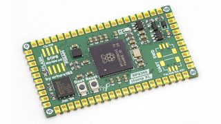
Every Raspberry Pi Pico 2 ships with 520KB of SRAM, but should a third-party wish, it can add up to an additional 16MB of PSRAM which also uses the QSPI interface (see the block diagram.) Pimoroni were quick off the mark to add 8MB of PSRAM to its Pimoroni Pico Plus 2 board which uses the RP2350B SoC. This board also has 16MB of external QSPI storage squeezed into a board that maintains electrical compatibility with the Raspberry Pi Pico 2.
If you need the RP2350B in a smaller form factor, but with the same 8MB of PSRAM and 16MB of QSPI storage, then Pimoroni’s PGA2350 offers an alternative. Measuring 25.4mm^, the PGA (Pin Grid Array) layout affords access to all 48 of the GPIO pins found on the RP2350B, all that you need to do is design a circuit around it.
An alternative to the PGA2350 comes from Solder Party. Its RP2350 Stamp XL breaks out all 48 GPIO pins of the RP2350B into a 45 x 25mm package. We get 16MB of QSPI flash, but only 520KB of RAM. The RP2350 Stamp XL is designed to be surface mount soldered to a carrier board, or to your own PCB project.
RP235X Availability
At the time of writing, the RP235X series are not in general circulation. There is obviously some quantity of chips available for third parties to design and sell their creations. But the RP235X is not for general sale as yet. It is hoped that the RP2350 will be in general circulation by the end of 2024.
The RP2354 is also mysterious; we’ve yet to come across a device with this chip inside of it. The RP2350 datasheet does provide details on the basic specs, but information such as the thermal characteristics have yet to be determined.

:quality(85):upscale()/2024/10/17/848/n/1922729/9dece426671163b35dcb11.60305022_.jpg)


 English (US) ·