
 11 hours ago
5
11 hours ago
5
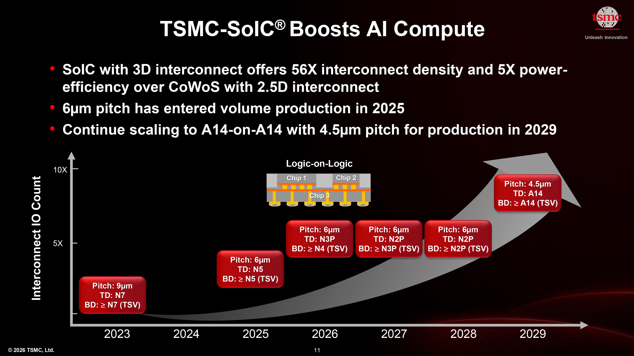
TSMC's chip-on-wafer-on-substrate (CoWoS) packaging technology has become the de facto standard packaging method for advanced AI and HPC processors that use HBM memory, thanks to TSMC's aggressive development of the technology. Unlike lateral 2.5D CoWoS, TSMC's vertically integrated System on Integrated Chips (SoIC) technology with 3D interconnects has not been adopted as widely. However, now that the company has overcome the first generation's constraints, it will aggressively develop this technology in the coming years, as the company revealed at its recent North American Technology Symposium.
Different kinds of stacking
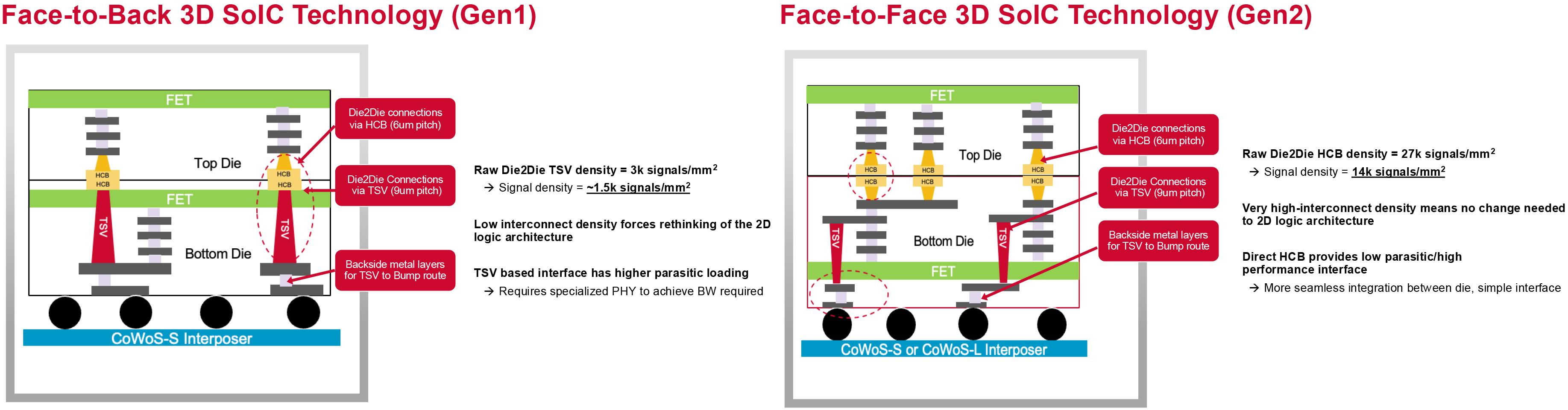
Face-to-back stacking imposes fundamental limits because signals cannot travel directly between dies. Instead, they must cross multiple metal layers and pass across through silicon vias (TSVs) in the bottom die, which increases latency, power consumption, and routing complexity.
Article continues below
In addition, this limits how densely connections can be implemented, since TSVs are relatively large structures that cannot be placed at fine pitch across active logic regions without affecting transistor density and design considerations. According to Broadcom, a real-world design using face-to-back stacking can achieve 1,500 signals/mm2 with TSVs.
By contrast, face-to-face stacking removes the indirect signal path by aligning the metal layers of two dies directly and connecting them using hybrid copper bonding. This enables straight, ultra-short vertical interconnects without relying on TSVs, which increases signal density by an order of magnitude to 14,000 signals/mm2, which therefore increases bandwidth, reduces latency, and cuts energy usage per bit.
As a result, communication between stacked dies resembles on-die wiring rather than chip-to-chip links, which is why companies like Broadcom view it as a crucial capability to scale compute density for next-generation AI and HPC processors.
3D packaging acceleration
Now that TSMC can do both F2F and F2B stacking, development of the technology will proceed much faster than before. The company now touts the usage of N3P dies on top of N4 dies, expects N2P on top of N3P within the next year, N2P on top of N2P by 2028, and envisions 3D stacked A14 dies by 2029.
Notably, the company hasn't demonstrated any process technologies with a backside power delivery in its SoIC roadmap. Yet, TSMC SVP Kevin Zhang reassured us that these nodes can support 3D integration as well.
"That may just be a simplification in the slide, A16 will have stacking capability," said Kevin Zhang, TSMC's Senior Vice President of Business Development and Global Sales, and Deputy COO.
"The SoIC roadmap shown does not cover all possible combinations — there are many permutations. The key takeaways are twofold. First, pitch scaling — from 9 µm to 6 µm, and eventually down to 4.5 µm. Second, the acceleration of stacking timelines. In the past, for example, you might stack N3P on N4, since the base die with TSV takes time to mature — 3nm TSV is only expected around 2027. But looking ahead to 2029, A14 TSV becomes available just one year after initial production. That shows how we are accelerating the schedule, enabling customers to stack the most advanced dies on top of each other much sooner."
The first face-to-face 3.5D designs
Being a leading developer of custom processors for hyperscalers, Broadcom is among the main users of TSMC's CoWoS and SoIC packaging technologies. Broadcom builds some of the world's largest system-in-packages, so it is not surprising that it is also among the first to use TSMC's F2F SoIC technology to build Fujitsu's Monaka supercomputer CPU.
On a high level, Fujitsu's Monaka processor is a heavy-duty general-purpose data center processor, and uses 144 Armv9 cores, spread over four compute chiplets made on TSMC's N2 technology, deploying a stacked face-to-face (F2F) atop dedicated SRAM chiplets (implemented on N5 technology) using hybrid copper bonding (HCB), equipped with a comparatively large I/O die that integrates the processor's memory controllers and PHYs for 12 DDR5 channels. Fujitsu's Monaka also features PCIe 6.0 connectivity with CXL 3.0 support for accelerators and memory expanders, as well as other interfaces expected from a modern data-center-class CPU.
Stacking N2-based CPU chiplets atop N5-made SRAM chiplets enabled Broadcom and Fujitsu to add massive amounts of cache to Armv9 cores to maximize their single-thread performance relatively cost-efficiently, but at the price of additional complexity and challenges surrounding thermals. Due to this, Broadcom and Fujitsu do not stack logic-on-logic, and it remains to be seen when TSMC's clients will actually start to use this option.
Broadcom is currently sampling Monaka with Fujitsu and aims to volume produce the CPU in 2027. Notably, while the company uses hybrid bonding, it also uses 9 µm pitches, which indicates that even innovators like Broadcom are cautious about using the latest versions of 3D integration technologies. This is in stark contrast to CoWoS, as TSMC's clients are eager to use the latest versions of the technology to build bleeding-edge processors.
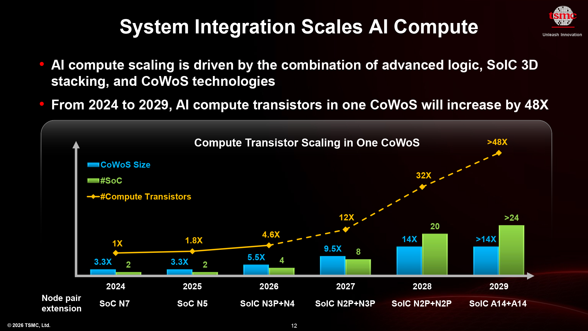
Nonetheless, TSMC clearly positions its SoIC 3D stacking as a way to increase compute density, so it clearly has reasons to expect this technology to be used widely. After all, if transistor scaling is slowing down, packaging is inevitably becoming the scaling engine.


 English (US) ·