
 1 month ago
33
1 month ago
33
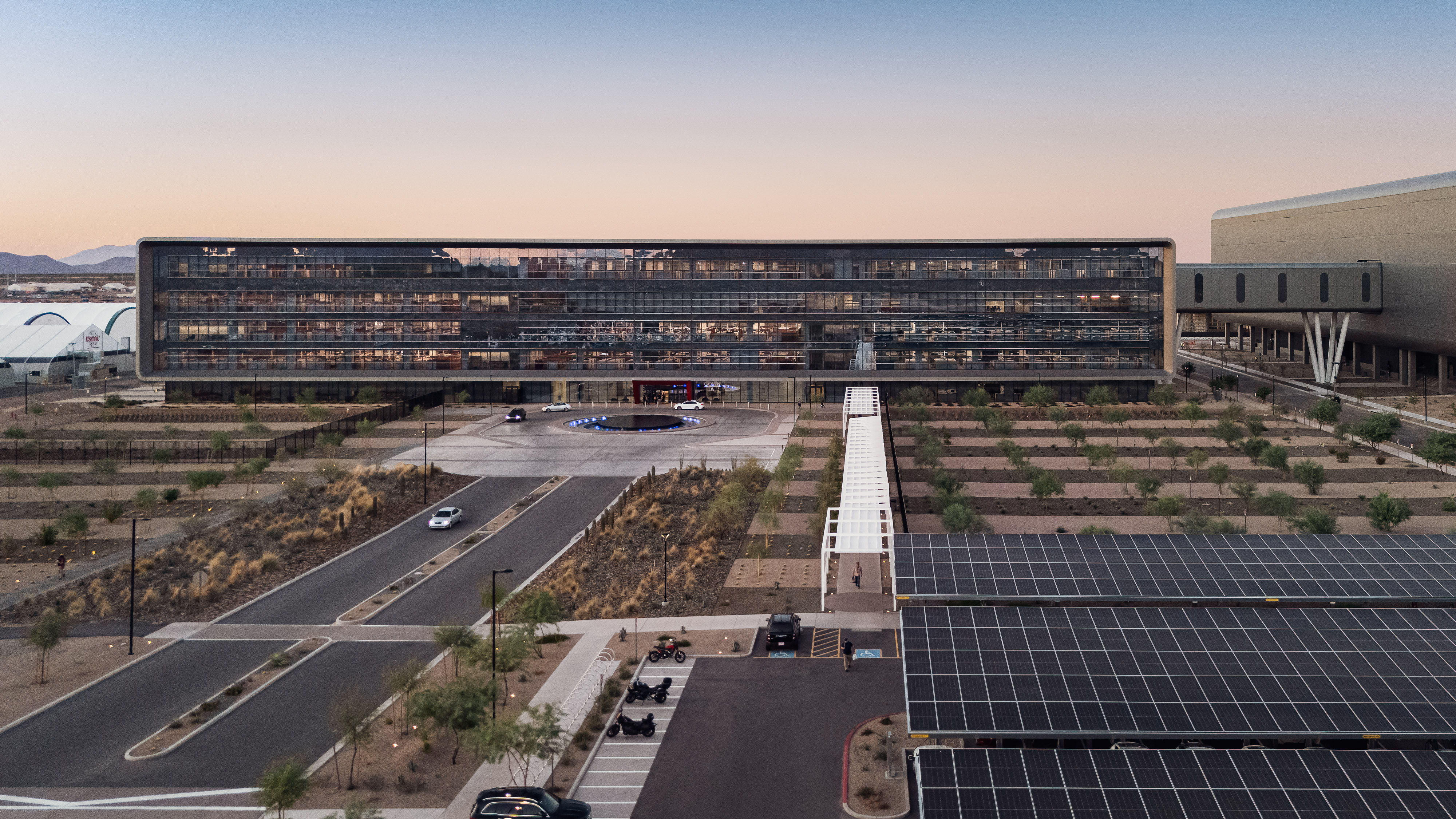
Taiwan Semiconductor Manufacturing Co. (TSMC) CEO C.C. Wei has said that it’s moving up its 2nm production plans in Arizona due to continued strong AI demand from its American customers. He also mentioned that the company is close to acquiring another massive property close to its latest fab in the U.S., hinting at a possible further expansion outside of its current $165 billion commitment, according to Nikkei Asia.
“We are preparing to upgrade our technologies faster to N2 and more advanced processes in Arizona, given the strong AI-related demand from our customers,” Wei said during a company earnings call. He also commented on the land acquisition, “Our plan will enable TSMC to scale up to an independent Gigafab cluster in Arizona to support the needs of our leading-edge customers in smartphone, AI, and HPC applications.”
TSMC has previously slowed its global plans because demand wasn’t there, but it has accelerated the development of its Arizona fabs because of robust demand from its U.S.-based clients. Construction of its N2 fabs at the site just started in April of this year, but it has already accelerated work on the site. The company initially expected chip production to begin by 2030, but this announcement will likely bring it up by around a year, although the company hasn’t mentioned a specific timeline yet.
Aside from that, the planned land acquisition hints at TSMC’s plan to turn its Arizona fab into a self-contained semiconductor manufacturing facility that can output 100,000 12-inch wafers monthly. This means having on-site packaging and testing alongside the fabs, with nearby supply chain partners and talent pipeline. In fact, the company has already begun working on developing future workers with its Arizona internship program, which has grown from 130 to 200 slots.

Follow Tom's Hardware on Google News, or add us as a preferred source, to get our latest news, analysis, & reviews in your feeds.


 English (US) ·