
 3 months ago
107
3 months ago
107
TSMC employees accused of stealing the foundry's trade secrets related to its upcoming 2nm-class fabrication process allegedly shared their findings with Japan-based foundry startup Rapidus, according to Money.UDN.com. The perpetrators reportedly shared 'hundreds of process integration technical photos' with the Japanese company, though their exact relationship with Rapidus is unknown and it is unclear whether the chipmaker asked for the said assets.
TSMC and the Intellectual Property Branch of the Taiwan High Prosecutors Office (THIP) are investigating a serious internal breach involving trade secrets related to TSMC's 2nm-class process technology. At least one current employee is suspected of working with a former colleague who now works at Tokyo Electron (TEL) to transmit sensitive data to Rapidus. There is no current evidence TEL was involved or was aware of the activity.
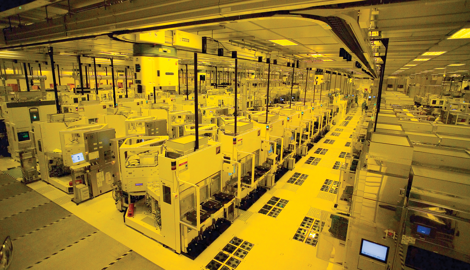
TSMC's internal systems flagged irregular activity, leading to an internal probe that confirmed exposure of corporate secrets. The suspected collaboration involves two individuals — one still employed at TSMC and another who moved to TEL , which is a supplier of both TSMC and Rapidus. The exchange between the two included 'hundreds of process integration technical photos,' which may have been used to fine-tune manufacturing tools essential for advanced node production, the report says. However, it is still unclear what kind of photos or pictures were shared.
Process integration activity combines individual process steps — such as deposition, etching, lithography, etc. — into a coherent flow that results in a working device. Typically, 'process integration technical photos' are highly detailed images or diagrams that show how various fabrication steps are combined into a complete and functional chip structure. Keep in mind that we are speculating here, as the report does not detail the contents of the images.
Such photos are considered extremely sensitive because they reveal proprietary process flows, design structures, layer materials, and integration techniques. They may expose key innovations such as gate-all-around transistors or specific patterning strategies, and offer deep insight into the particular production node — and even the company's capabilities in general. However, given how complex modern process technologies are, such images can — even though they are sensitive — barely serve as a blueprint for process development or integration. However, they can certainly help to fine-tune tools (at least some tools, and only to a certain degree).
Rapidus claims that it co-developed its 2nm-class manufacturing technology with IBM (for what IBM got into a legal action with GlobalFoundries) and is currently conducting trials of the production node. The technology is expected to enter mass production in 2027.
Since TSMC's and Rapidus's 2nm-class production nodes are different and the two companies even have different views on how wafers should be processed, it is unlikely that the foundry could get a lot of useful information for its fab from TSMC's 'process integration technical photos.' However, such information could give an idea to competitive analysis teams about what TSMC's N2-series fabrication technologies are about.
Keep in mind that the reports about employees stealing TSMC's 2nm-related trade secrets are vague (to put it mildly), and should be taken with grain of salt. While the initial reports said that up to six people were involved in the wrongdoing, the new report claims that there were 'around' 10 perpetrators. Also, the initial reports failed to detail what information was stolen from TSMC, and the new report mentions 'hundreds of process integration technical photos,' but does not disclose what was on those images.
For now, it is hard to evaluate what exactly happened or assess the possible damage to TSMC and/or benefit to Rapidus (if any).


 English (US) ·