
 3 weeks ago
133
3 weeks ago
133
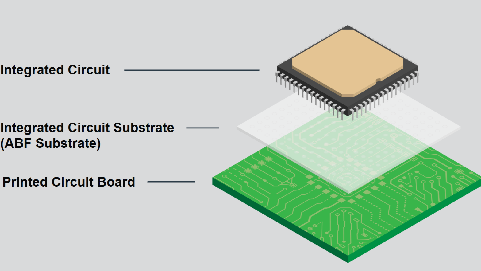
ABF substrates, the specialized insulating and wiring bases that connect tiny silicon chips above them to the much larger printed circuit boards below, sit beneath most high-end CPUs, GPUs, and AI accelerators. Featuring the Ajinomoto build-up film (ABF), these substrates have been critical to the semiconductor industry since the late 1990s, with personal computers, workstations, servers, and networking silicon driving steady demand for decades.
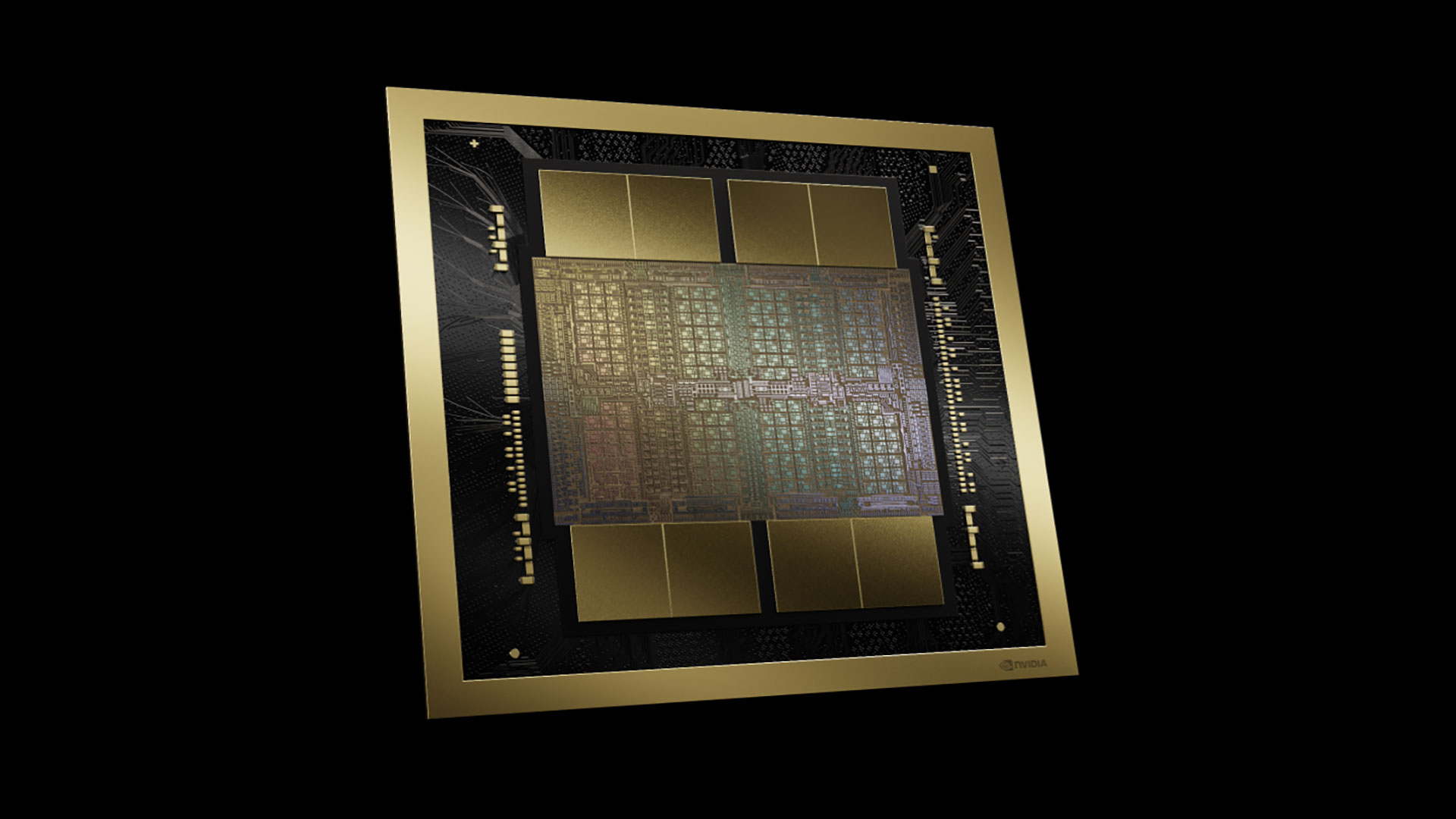
The artificial intelligence boom has multiplied that demand exponentially. Training and inference for frontier models now run across data centers, each housing hundreds of thousands of accelerators and providing hundreds of megawatts of compute. Nvidia alone shipped an estimated 3.2 million Blackwell GPU packages through the end of 2025, with every one of those accelerators packaged on an ABF substrate. Meanwhile, the industry is already entering the gigawatt era with humongous data center buildouts, each expected to house millions of AI accelerators.
This edifice rests on a remarkably narrow supply chain. Practically every advanced logic and AI chip made today by Intel, AMD, and Nvidia depends fundamentally on ABF substrates. These substrates are the conventional default for high-performance packaging. They are made by a small group of specialists, including Unimicron, Ibiden, Kinsus, Shinko Electric Industries, Samsung Electromechanics, and Nan Ya PCB. The upstream supply chain gets much tighter.
The one common denominator across ABF substrates, regardless of manufacturer, is the Ajinomoto build-up film itself. Each substrate maker laminates its build-up layers using dielectric film supplied by Japan's Ajinomoto, which controls a reported 95% or more of the global market. A single company, better known for food seasoning than microelectronics, sits at the base of one of the most concentrated supply chains in computing, almost singlehandedly supplying a material for hundreds of millions of semiconductor devices. Not surprisingly, demand is now growing beyond what the supply chain can comfortably supply.
Compounding this crunch, modern AI accelerators now pack multiple compute, memory, and supporting components onto a single board. As a result, the substrate is getting larger across the X-Y footprint to accommodate the expanding package. Manufacturers are also adding more build-up layers to the substrate to route the growing number of signals and power connections. Each additional layer requires another ABF layer, further multiplying demand across millions of accelerators and extending manufacturing times.
Unfortunately, the complications don't stop there. Beyond further straining the supply chain, expanding the substrates is creating technical problems, such as warpage, yield issues, and electrical losses within the component itself. This leaves the ABF substrate ecosystem facing two related challenges: producing enough advanced substrates for a rapidly expanding fleet of AI accelerators, while simultaneously re-engineering these substrates so they can continue to scale without becoming unmanufacturable or impractical.
The ABF substrate roadmap is consequently as much about supply-chain capacity as it is about the hardware itself, with suppliers such as Ajinomoto and Ibiden outlining plans to expand material and manufacturing capacity, respectively. At the same time, the wider industry — Intel, Samsung, and SK's Absolics among them — is exploring glass-core substrates and other material technologies to push past the limits of organic ABF.
ABF substrates
Silicon dies, including CPUs and GPUs, cannot communicate directly with the printed circuit board beneath them. The connection pads on a die are spaced micrometers apart, while the traces on a motherboard are spaced hundreds of micrometers to millimeters apart. Every high-performance chip, therefore, sits on an intermediary package substrate — a dense, multilayer board that fans the ultra-fine connections on the die outward into connections large enough for the motherboard to handle, while also providing signal routing, power and ground distribution, and mechanical support for the package.
ABF substrates used in AI accelerators typically consist of a rigid, glass-reinforced resin core sandwiched between successive build-up layers of copper wiring and insulating film. The core provides much of the mechanical rigidity, while the layers provide the increasingly dense wiring required close to the silicon.
To create the substrate, the manufacturer laminates the ABF dielectric onto the structure, forms microscopic vias — commonly with a CO2 laser — and then uses lithography and copper deposition to create a new wiring layer. High-end substrates typically use a semi-additive process (SAP), in which fine copper traces are plated up from a thin conductive seed layer. Another ABF layer is then laminated over it, and the process repeats. The film electrically separates successive copper layers, while plated microvias connect them vertically.
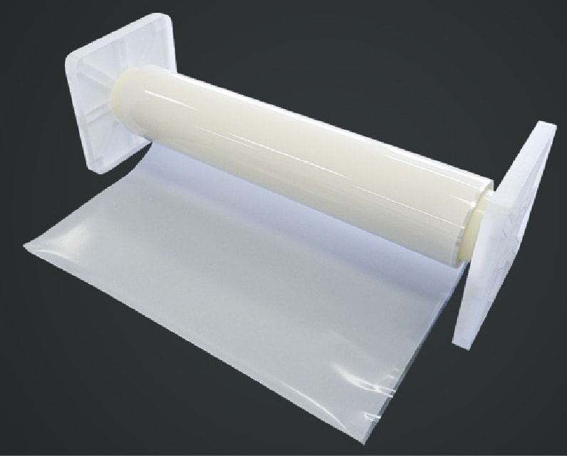
Ajinomoto developed the film in the 1990s, after which it gradually became the industry default for its low dielectric loss, fine-line capability, and smooth lamination. The company reportedly accounts for roughly 95% of the substrate film market, with its nearest competitor, Sekisui Chemical, holding only a low-single-digit share.
The manufacturing tier above the film is more populated but still concentrated. Unimicron, Ibiden, and Shinko together account for roughly three-quarters of the substrate market by most estimates, with AT&S and Nan Ya PCB rounding out the leading group. These companies take ABF and other materials and manufacture the finished multilayer substrate. Semiconductor packaging companies, such as TSMC and Amkor, then integrate those substrates into packages containing the processor, memory, and other components.
AI accelerators are pushing substrates outward and upward
To deliver the compute and memory bandwidth that frontier models demand, the industry is packing ever more silicon onto each AI accelerator. Designers now place multiple large logic dies alongside a growing number of high-bandwidth memory stacks on a single package. Nvidia's Blackwell generation mounts two reticle-sized GPU dies and eight HBM3E stacks on a single package, with its upcoming Rubin and Rubin Ultra parts pushing it further still. TSMC's CoWoS packaging is scaling from around 3.3 reticles — each roughly 830 square millimeters of silicon — a generation ago to 5.5 reticles in volume production in 2026, with a roadmap reaching 9.5 reticles in 2027 and beyond 14 reticles by 2029, when a single package is expected to carry roughly ten compute dies and twenty or more memory stacks.
This expansion of the accelerator package is driving the substrate’s expansion on two physical levels. The first expansion is the substrate's footprint in the X-Y axes. The base has to get wider and longer to accommodate the larger package footprint. Ibiden's current roadmap puts its cutting-edge substrate size at 90 × 90mm (3.54 x 3.54 inches) in 2026, 110 × 110mm (4.33 x 4.33 inches) in 2028, and 130 × 130mm (5.12 x 5.12 inches) and larger from 2030 onward. Ajinomoto independently expects the representative advanced AI packages its film goes into to grow from roughly 100 mm² in 2026 to about 120 mm² for 3D AI packages from 2031.
The second expansion is along the Z axis through additional layers. An expanded collection of compute dies and memory creates more signals to route, while the corresponding increase in power draw requires extensive power and ground distribution, all of which must be carried in a growing number of layers. Ibiden's roadmap targets a 10-X-10 buildup structure in 2026, 12-X-12 in 2028, and 14-X-14 from 2030. Here, the numbers represent the build-up layers on either side of the central substrate core: “10-X-10” means 10 build-up layers per side of the core — which is represented by the “X” — each comprising one dielectric layer (ABF) plus one patterned copper layer, working as a pair.
Nan Ya PCB's roadmap points in the same direction. From an 11+N+11 baseline, it targets 24-layer substrates in 2026 and more than 24 layers in the first half of 2027, while tightening line and space from a 9/12 µm baseline to 8/8 µm and then to 6/7 µm by early 2027. Layer-counting conventions differ between vendors, so a per-side figure and a total layer count don't necessarily line up directly.
The substrate’s expansion in both directions creates several challenges. Increasing the X-Y area makes the package harder to keep flat. Silicon, copper, the substrate core, and the polymer build-up materials that make up the substrate expand by different amounts when heated. As the package is bonded during assembly at around 250⁰C and then cooled, these mismatches cause the layers to pull against one another, leading to warping — a problem that becomes harder to control as package dimensions increase.
Excessive warpage can undermine solder-joint formation, layer-to-layer alignment, and reliability, while a larger substrate also occupies more manufacturing-panel area and exposes more area to potential defects. Organic substrates are reported to lose usable flatness once packages exceed roughly 120mm per side, a threshold that the largest AI accelerators are now reaching and that Ibiden's own roadmap — climbing toward 130mm and beyond — is set to cross.
The growing layer count along the z-axis also creates manufacturing challenges around yield, capacity, and time. Every new substrate layer requires a full manufacturing sequence of several steps, all held to sub-ten-micron tolerances. Each added layer increases the chance of a defect or alignment error that can scrap the whole substrate.
Additionally, layer count consumes manufacturing capacity and time in proportion. This is why Ibiden frames future demand in terms of semi-additive processing load rather than a simple substrate count, as a single advanced substrate now consumes far more of a line's capacity than a finished-unit tally would suggest.
Overall, the simultaneous expansion in substrate area and layer count means ABF consumption is rising much faster than processor shipments alone suggest. Ajinomoto illustrated this in its 2025 integrated report with a larger AI substrate that had about 3.5 times the board area and three times as many ABF layers as a conventional design — 18 layers against six — consuming roughly ten times as much ABF overall. This surging material consumption, set against an extremely concentrated supply base, extends the ABF substrate story beyond a technical problem into a supply-chain constraint.
The supply chain constraint
Like many components in the semiconductor industry chain before the AI boom, demand for ABF substrates periodically swung both ways. A severe bottleneck through 2020-2022 — driven by pandemic-era PC and server demand — was followed by an oversupply in 2023, as substrate manufacturers expanded capacity. However, that capacity was built for low-layer-count, smaller consumer substrates, not the large-body, multi-layer packages AI demands.
These advanced products require sufficiently large manufacturing formats, fine SAP wiring, tight layer registration, acceptable warpage, and high yields across much larger structures. Ibiden captures this by measuring demand not in finished substrates but in semi-additive-process load — the actual processing work each part imposes on a line. Indexing 2024 at 1.0, it expects the SAP load of a single AI-server substrate to reach 1.8 times that in 2026 and 2.5 times in 2028, with the company stating that substrate expansion will push total SAP demand beyond industry supply capacity, indicating a constraint in the manufacturing process itself.
The bottleneck is even tighter at the ABF material level. Ajinomoto's film capacity was already running at full load in the second quarter of 2026, at a reported two million square meters per month, although the company has outlined plans to increase capacity. A near-monopoly supplier at full capacity while consumption surges paints a clear picture of the bottleneck’s severity.
Unsurprisingly, prices have moved accordingly. Ajinomoto notified substrate manufacturers in May 2026 that it would raise ABF film prices by approximately 30%, effective in the third quarter. The hike is coming alongside comparable increases in copper-clad laminates from Resonac and Mitsubishi Gas Chemical, compounding pressure across the whole stack. Further tightening the squeeze, Ajinomoto recently cut shipments of the critical ABF film to China by 30%.
The growing ABF substrate problem cannot simply be attributed to Ajinomoto running out of film. In fact, while it's running at full capacity, the company says it has no concerns about its overall supply chain. The constraint stretches across the entire chain containing ABF, glass cloth, and other materials, SAP equipment, large-format substrate factories, yield, and customer-qualified production capacity.
The immense industry demand is progressively tightening the crunch. Several supply-chain analyses converge on an ABF supply-demand shortfall of roughly 10% in the second half of 2026, widening to around 21% in 2027 and potentially exceeding 40% by 2028, with demand for substrate area projected to grow at a compound annual rate near 39% from 2025 to 2028 as accelerators integrate more components.
The roadmap to recovery: more capacity, better materials
The industry is responding to ABF substrates' multifaceted constraints on multiple fronts: expanding manufacturing capacity to relieve near-term supply pressure while qualifying new materials and substrate architectures to break through the technical limits. Capacity expansion is already underway across the supply chain.
Ibiden is executing ¥500 billion ($3.1 billion) in capital investment across fiscal years 2026 to 2028 — the largest single substrate expansion on record — targeting 2.8 times its 2024 capacity for ASIC and AI-server substrates by 2028. Unimicron raised its 2026 capital spending to a record NT$34 billion ($1.07 billion), with a focus on ABF substrates. Meanwhile, Samsung Electro-Mechanics, Samsung's substrate arm, has committed $1.2 billion to expand ABF substrate production, with volume production expected by the third quarter of 2027.
Pegatron's substrate unit, Kinsus, has approved NT$23.5 billion ($722 million) for ABF equipment over three years and now focuses its most advanced lines almost entirely on AI clients, aiming to lift monthly output at its Taoyuan plant by roughly 25% by 2027. While these projects address the shortage directly, their lead times mean the crunch may continue for a while, as supply cannot respond instantly to the AI demand spike.
Ajinomoto is expanding upstream as well. A new plant in Gunma entered full operation in 2025. The company has invested roughly ¥25 billion ($157 million) in ABF production since 2023 and has said it will invest at least as much again by 2030, targeting a capacity increase of more than 50%. It is also adding a third Japanese base for varnish production — envisioned to provide capacity comparable to Gunma — with construction planned for 2028 and operations to begin in 2032.
However, capacity only solves the problem if the current substrate architecture can continue to scale. The material roadmap — aimed at addressing the physical constraints of ABF substrates — is therefore advancing parallel to the factory roadmap. Ajinomoto says present and future ABF generations are being engineered for larger, more multilayered substrates, high-bandwidth I/O, lower transmission loss, and improved resistance to warpage and humidity. The company expects newer, higher-value ABF grades to take an increasing share of its portfolio through 2030.
Substrate makers are addressing the problem from the process side. Nan Ya plans to move beyond 150 mm body sizes and 24 layers while shrinking copper line/space geometry toward 6/7 microns in the first half of 2027. Its materials roadmap includes an ultra-low-CTE core material with a CTE below 3 ppm/°C, alongside low-Dk, low-Df, and low-CTE dielectrics. Finer wiring allows a substrate to support more connections without relying solely on additional area or layers, while low-expansion materials help keep the growing structure flat.
Eventually, the substrate's central core itself may change to glass. Organic substrate cores are increasingly difficult to keep dimensionally stable as packages approach and surpass 100 mm. Glass can be matched more closely to silicon's thermal expansion — providing dimensional stability — and offers substantially lower dielectric loss for high-speed links. It has therefore emerged as one of the industry's main solutions to warpage.
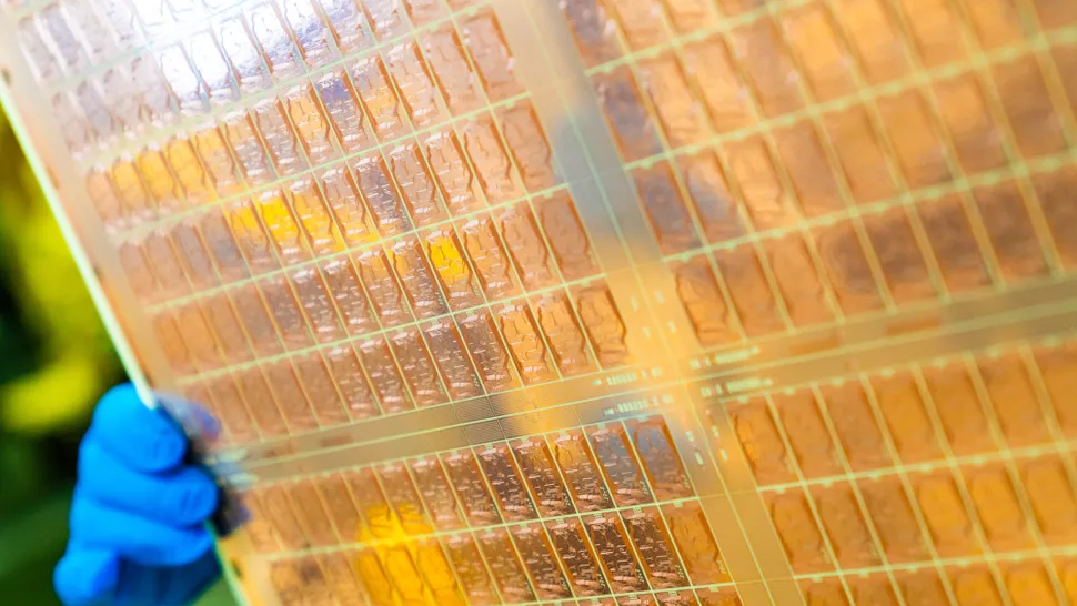
As we detailed in our glass substrate roadmap, the move to a glass core is drawing a broad field, as it sits at the intersection of substrate-making, glass manufacturing, and advanced packaging, pulling in chip-and-packaging houses, display and glass specialists, and the incumbent substrate makers alike. Intel demonstrated a package that combines EMIB with a glass substrate at NEPCON Japan in January 2026, although the company still places commercial glass-substrate deployment in the latter half of the decade.
SK Group subsidiary Absolics is operating a low-volume glass-substrate manufacturing facility in Covington, Georgia — backed by $100 million in US CHIPS Act funding — producing prototype and qualification samples for customers, such as AMD for its MI400-series accelerators, while Samsung Electro-Mechanics is producing prototypes on a pilot line in Sejong and now plans mass production through its glass-core joint venture after 2027.
TSMC, meanwhile, is pursuing panel-level packaging through its chip-on-panel-on-substrate (CoPoS) platform, moving to a 310 x 310mm panel format, with a pilot line at its VisEra subsidiary, trial production targeted for 2027 and mass production for the second half of 2028. Glass-core substrates are a separate, later step on TSMC's roadmap, with commercial scale projected after 2030. Ibiden also puts “glass core” on its substrate technology roadmap around 2030 as a solution for warpage control.
The glass core — most likely a late-2020s-to-2030s technology — is positioned as a solution to the warpage wall. It replaces the organic core, not the ABF itself, which would remain the buildup material. A glass core may soften ABF demand per package, as glass's flatness allows finer routing and potentially fewer buildup layers, but it does not remove the material or the dependency. There's the possibility that a future dielectric material will eventually replace ABF, although that doesn't seem to be the industry's main focus currently.
Regardless, the near-term roadmap centers on more advanced SAP capacity, rapidly expanding factories, improved materials, and increased supply. Through the late 2020s, finer wiring, lower-loss ABF, lower-CTE materials, and better warpage control will enable organic substrates to stretch toward 110 mm and beyond. Around 2030, glass cores offer a path toward the 130 mm-plus packages that Ibiden and others already have on their roadmaps.



 English (US) ·