
 2 hours ago
4
2 hours ago
4
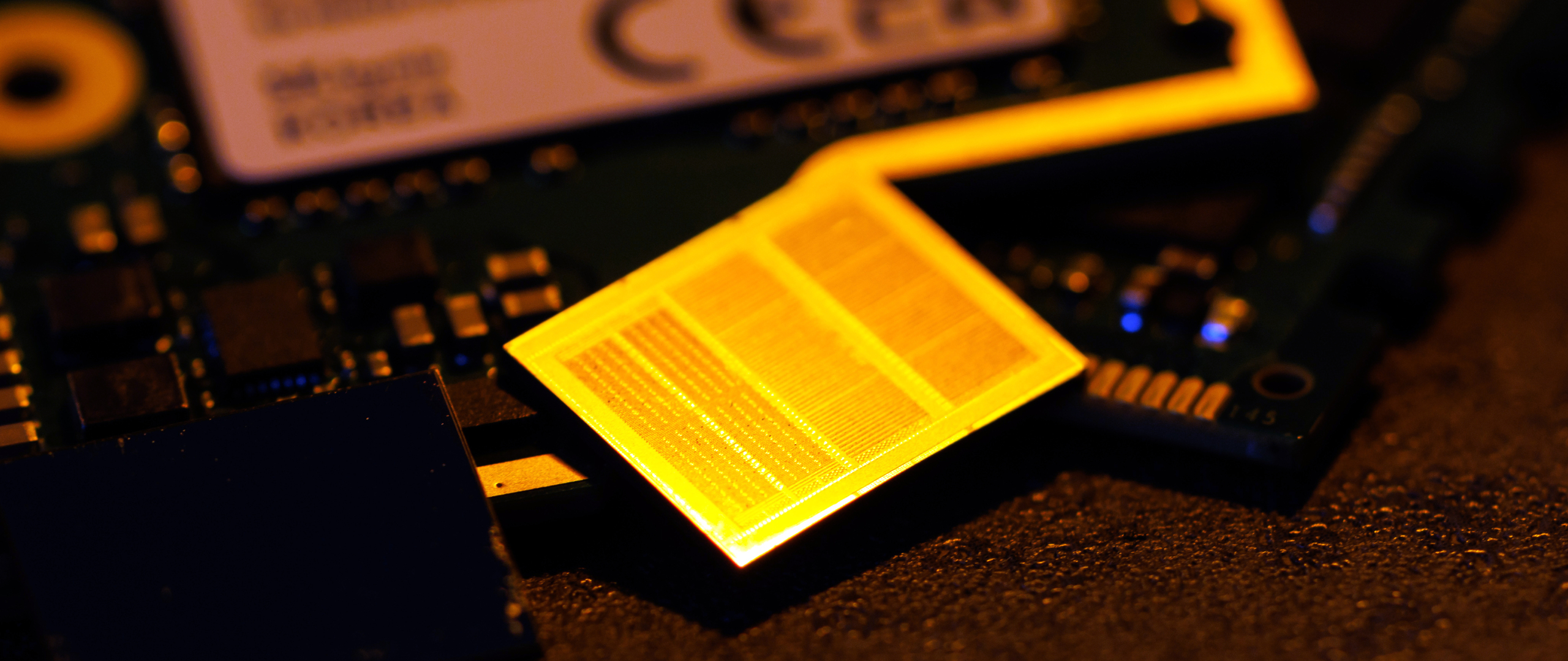
Hybrid bonding, the copper-to-copper joining technique that replaces solder microbumps in 3D chip stacks, is in high-volume production on logic chips and has just been postponed for use with memory. TSMC has scaled its SoIC bond pitch from 9 microns to 6 and laid out a path to 4.5 by 2029; Intel began shipping Foveros Direct hybrid bonding in its Clearwater Forest server CPU in the first half of 2026, and AMD has used the technology in volume since the first 3D V-Cache parts. However, a JEDEC decision earlier this year to raise the HBM stack-height limit lets HBM4 stay on the less sophisticated and expense microbump technology, deferring hybrid bonding's arrival in high-bandwidth memory, and is now set to debut in HBM4E and HBM5 at the end of the decade.
The technique works by polishing two dies flat, then bonding their copper pads and surrounding dielectric directly under heat and pressure, with no solder bump in between. Because there’s no bump to collapse, the connections can be packed far tighter. AMD has cited roughly 15 times the interconnect density of conventional 2.5D microbump stacking, and figures presented at TSMC's 2026 technology symposium put face-to-face hybrid bonding at around 14,000 signals per square millimeter against roughly 1,500 for face-to-back through-silicon-via stacking.
Wafer-to-wafer, die-to-wafer, and throughput
Microbumps have historically run at pitches around 40 microns, tightening toward 10 for the latest memory. Hybrid bonding, however, starts where microbumps end and keeps scaling: the leading edge is at 6 microns now, with 4.5- and 3-micron generations in development and sub-micron pitches demonstrated in research. Each step down multiplies the number of vertical connections between stacked dies, allowing a cache die or a compute tile to behave as if it were part of the chip rather than a separate component wired across a package.
The method is split into two different approaches: wafer-to-wafer and die-to-wafer. Wafer-to-wafer bonding joins two full patterned wafers face-to-face and dices them afterward, which allows the tightest pitch and fastest production because alignment happens once at the wafer scale. Imec and EV Group demonstrated a 200-nanometer wafer-to-wafer pitch with post-bond overlay below 40 nanometers at ECTC in May. The constraint here is that both wafers must carry identically sized dies, and every die gets bonded, including defective ones, so a single bad die on either wafer ruins the pair.
In contrast, die-to-wafer bonding places individual, pre-tested dies onto a wafer — which is what chiplet and HBM stacks require — because it allows known-good-die selection and the mixing of different die sizes and process nodes. There’s a penalty in terms of throughput with die-to-wafer as each die is picked, aligned, and placed in sequence rather than in one wafer-scale step.
The best die-to-wafer pitch shown at ECTC 2026, from CEA-Leti, was 1 micron, roughly five times looser than the wafer-to-wafer record. Because the dies are placed one at a time, the speed the bonder runs at sets the limit on how many chips it can produce. Applied Materials and Besi cite around 1,600 die placements per hour on the Kinex platform, and Besi's Chameo bonders are rated near 2,000 chips per hour, with the next generation aiming for 50-nanometer placement accuracy to reach finer pitches.
Hybrid bonding is difficult to achieve, as two surfaces have to be almost perfectly flat and clean. The dielectric holds on contact through van der Waals forces, so the polished surface can vary by no more than around 0.2 nanometers, and the copper pads have to sit a few nanometers below it, close enough that they swell into contact when the stack is heated to 200 to 300℃. A single particle smaller than a micron holds the surfaces apart and leaves a gap spanning many pads at once. So keeping the wafer clean and flat through the polishing step (known as chemical-mechanical planarization) is critical for good yields.
TSMC SoIC and Intel Foveros Direct
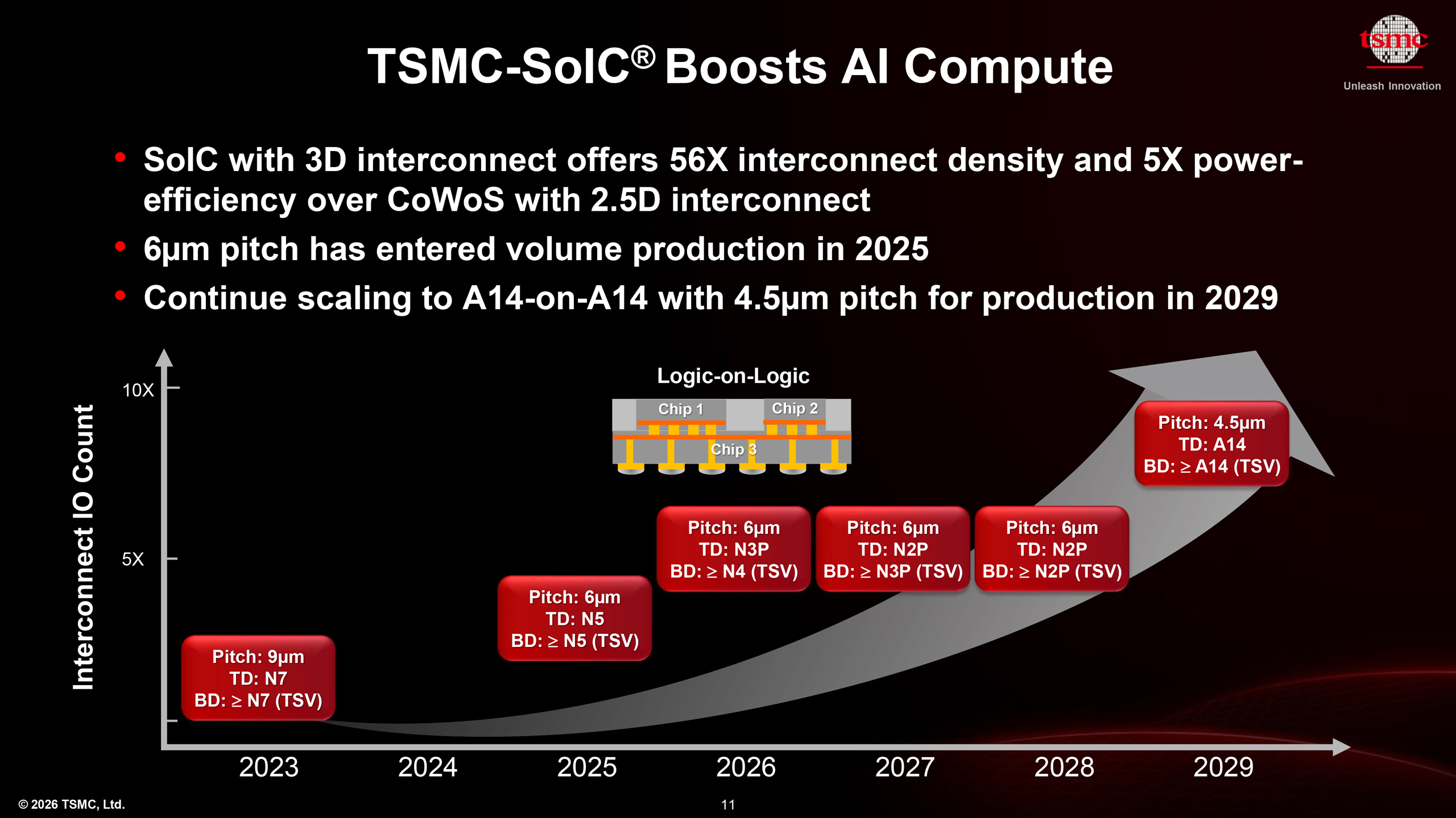
In terms of who’s leading hybrid bonding, TSMC’s System on Integrated Chips (SoIC) platform leads in terms of volume. At its 2026 North American Technology Symposium, the company laid out a pitch roadmap moving from 9 microns in 2023 to 6 microns in 2025 and 4.5 microns by 2029, with second-gen SoIC adding face-to-face bonding on top of the face-to-back stacking that the first generation supported. The node-stacking roadmap runs in parallel, from N3P-on-N4 today toward N2P-on-N2P by 2028 and A14-on-A14 by 2029.
With SoIC, the hybrid-bonded stack is built first as a vertical block, then placed into a CoWoS module alongside HBM on a silicon interposer, a combination the industry calls 3.5D. AMD's MI300 is the reference case, stacking compute and I/O dies by hybrid bonding before the assembly is mounted in CoWoS with its memory. SoIC handles the front-end vertical density; CoWoS handles the back-end lateral integration with memory.
Capacity is slowly growing, with TSMC building out its Chiayi AP7 site as its largest advanced-packaging campus. Output is targeted for 2026, and analysts at TrendForce have estimated SoIC capacity roughly doubling year on year from a few thousand wafers a month in 2024. Customers include AMD, whose 3D V-Cache and MI300 accelerators were the first volume SoIC products, and the Broadcom-built Fujitsu Monaka CPU.
Meanwhile, Intel's hybrid-bonding implementation, Foveros Direct, reached high volume with Clearwater Forest, the Xeon 6+ server processor built on the 18A node and demo’d at MWC back in March. The design uses a 9-micron copper-to-copper pitch to bond compute and I/O tiles onto base tiles that act as an active interposer, and Intel has described a second generation targeting a 3-micron pitch. Enabling that on a leading-edge logic node required a dedicated process variant, 18A-PT, which adds the through-silicon vias (TSVs) and bonding support that standard 18A doesn’t carry. The shift from Intel's earlier Foveros, which used solder microbumps across the Ponte Vecchio GPU's chiplets, to direct copper bonding is a generational change now playing out across its server offerings.
The unexpected HBM delay
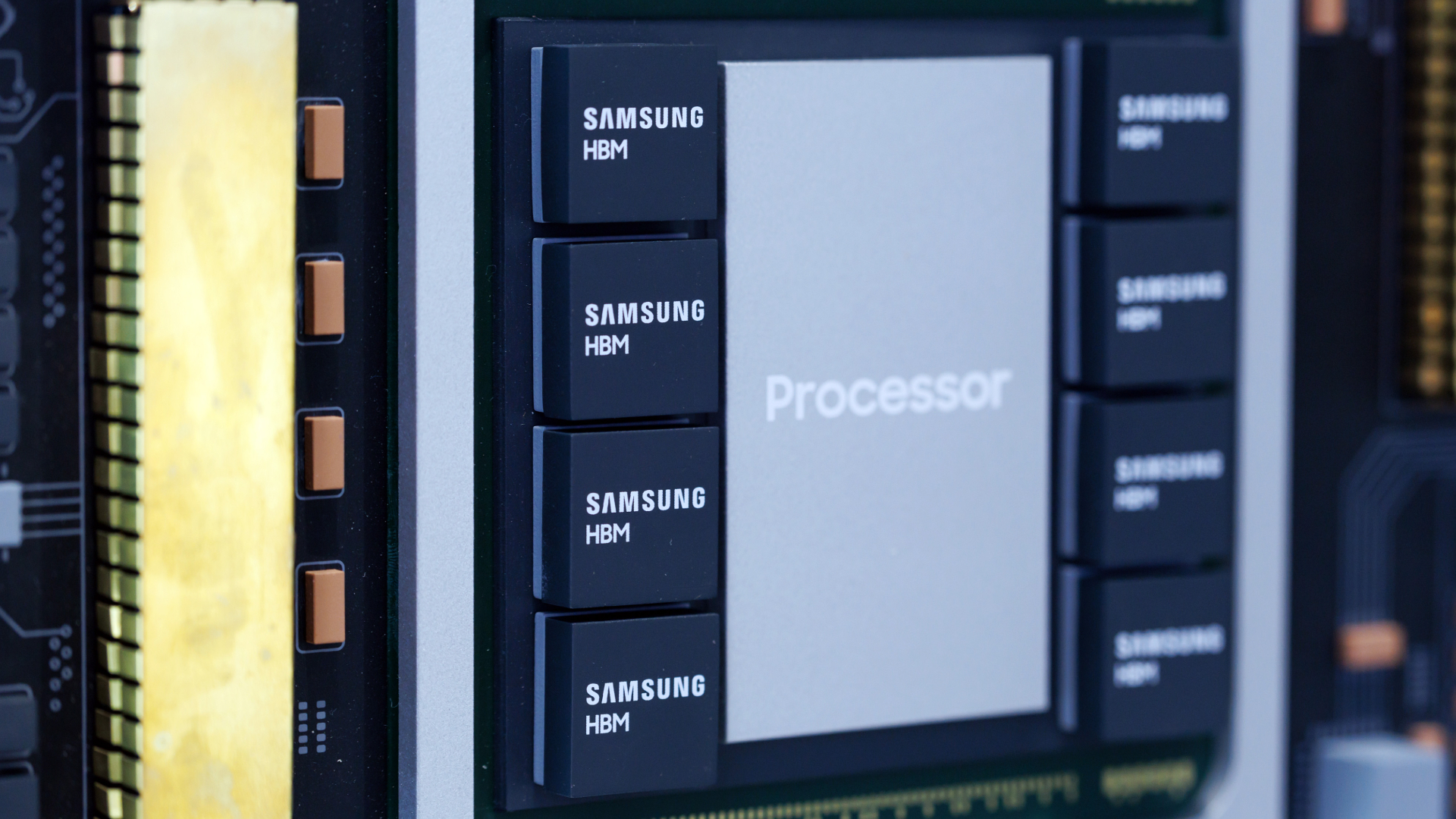
The widely held assumption was that HBM, the stacked DRAM that sits beside every AI accelerator, would be hybrid bonding's largest market by volume. That changed back in January when JEDEC raised the HBM package height limit from 720 to 775 microns, and the extra room means 16-high HBM4 stacks can be assembled with microbumps after all. With HBM4 pad pitch at 10 microns, reporting from SemiEngineering noted that moving to hybrid bonding at that pitch wouldn’t yet make economic sense.
SK hynix has reflected that logic in its own planning, reportedly sticking with advanced mass-reflow molded underfill for 16-high HBM4 while keeping hybrid bonding as a backup and continuing to validate 12-high hybrid-bonded samples for later generations. The company demonstrated a 16-layer HBM4 sample at CES 2026, built without the all-hybrid bonding many expected the generation to require. The result pushes hybrid bonding's HBM debut toward HBM4E and HBM5, expected around 2027 to the end of the decade, where taller stacks and tighter pitches finally make the older bonding methods run out of room.
Meanwhile, the memory makers are building the packaging capacity regardless. SK hynix is investing $3.87 billion in an advanced-packaging plant in Indiana, with production targeted for 2028, and Micron broke ground on a $7 billion HBM advanced-packaging facility in Singapore early last year, with output expected around 2027. Those plants are sized for the volumes hybrid bonding will eventually carry, even as the first HBM4 generation ships on the older interconnect, meaning the equipment commitments are running ahead of the technology's confirmed deployment date in memory.
Samsung is doing the same thing from the memory side. Its SAINT packaging family includes SAINT-D, which stacks DRAM directly on a logic die, and the company has discussed a bufferless HBM4 design that removes the separate base die, with custom HBM logic dies reportedly moving to its 2nm foundry process for 2027 samples. At GTC in March, Samsung claimed hybrid bonding cuts thermal resistance by more than 20% against thermocompression bonding.
Another drag on the timeline is intellectual property. Adeia, which holds a large portfolio of bonding patents, sued AMD last year, alleging that the hybrid bonding behind 3D V-Cache infringes 10 of its patents.
China is pursuing the technique as a way around its lack of access to cutting-edge lithography. With SMIC limited to 14nm-class production and cut off from next-gen EUV, domestic researchers have identified 3D hybrid bonding as a route to competitive performance by stacking older logic and DRAM, with public claims of 14nm parts paired with domestic DRAM aimed at rivaling far newer GPUs. Given that it’s China we’re talking about here, those claims remain claims, and no foundry has demonstrated mass production of hybrid-bonded logic memory in China.
In terms of tooling, Applied Materials and Besi, partners on hybrid-bonding equipment since 2020, launched their Kinex die-to-wafer bonding system late last year, billed as the first fully integrated die-to-wafer hybrid bonder combining surface preparation, bonding, and metrology. Applied Materials has taken an equity stake in Besi, and reports from March placed Besi at the center of takeover interest from both Lam Research and Applied Materials, an indication of how important the bonding-tool market has become as logic adoption ramps and memory adoption is staged behind it.
Analyst tracking put Besi’s hybrid-bonding revenue on a path toward roughly €476 million by 2026, up from about €36 million in 2023, with second-half 2025 orders rising more than 60% against the first half on early HBM4 production-line bookings. Competing tool vendors are moving in alongside it: ASMPT has partnered with EV Group on hybrid bonding, and SK hynix is working with Hanwha Semitech on bonders targeting a commercial HBM launch in 2027. The sheer scale of this equipment build-out is a clear demonstration that the industry is treating hybrid bonding as an inevitability, even where the products that’ll use it are still years out.
Hybrid bonding is already in volume production, but its capability is outpacing its adoption. TSMC offers 6-micron pitch while its newest disclosed customer ships at 9; Intel ships at 9 with 3 on the roadmap; and the memory market that was meant to consume it in quantity has bought itself one more generation on microbumps. Two things will show where it goes next — whether any leading logic product drops below 9 microns in volume, and whether HBM4E marks hybrid bonding's first real use in memory before the end of the decade.






 English (US) ·