
 5 hours ago
5
5 hours ago
5

SK hynix, TetraMem, and researchers from the University of Southern California have developed a memristor-based in-memory computing (IMC) system-on-chip (SoC) for AI edge devices. The device is designed to accelerate neural network inference in lightweight AI models while consuming a fraction of the power that higher-end GPUs or NPUs would. To a large degree, the SoC is a proof-of-concept chip, as its performance would peak at around 2.54 TOPS in a theoretical best-case scenario, which is 16X below Microsoft's Copilot+ requirements.
A DWC-optimized IMC architecture
Memristor-based in-memory computing (IMC) accelerates neural networks by performing analog computations directly inside memory arrays, which reduces data movement and power consumption. However, depthwise convolution (DWC) — a core operation in lightweight networks such as MobileNet — performs independent per-channel filtering with limited data reuse and therefore maps poorly onto conventional crossbar arrays. To address this limitation, researchers from SK hynix, TetraMem, and USC developed an SoC that features both conventional IMC crossbars and a memristor-based IMC architecture specifically optimized for DWC.
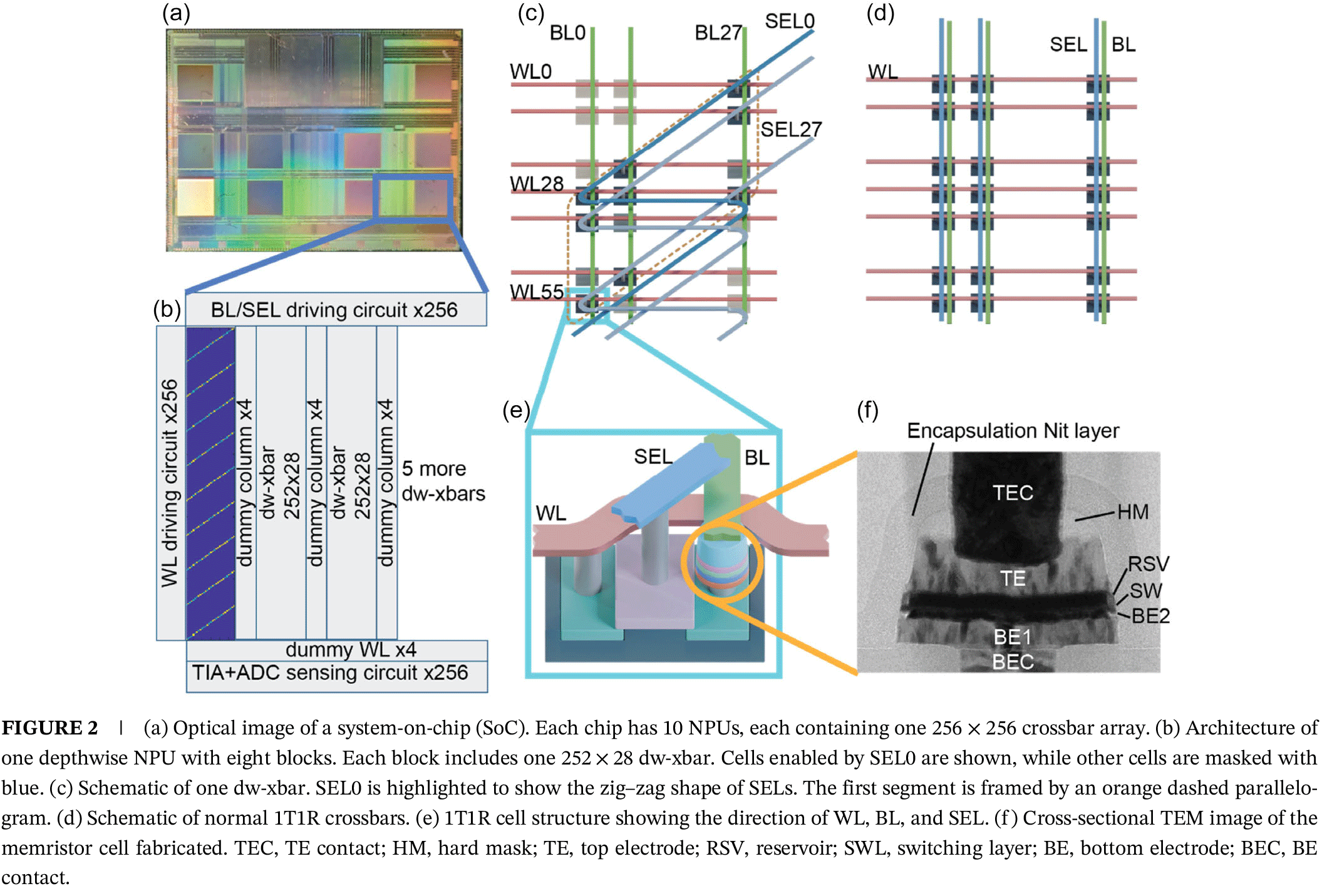
The jointly developed SoC is based on an embedded RISC-V processor that schedules workloads and features 10 neural processing units (NPUs). One NPU out of 10 is dedicated to depthwise convolution, while the remaining nine execute pointwise and dense operations. Nine out of 10 NPU include a 256 × 256 memristor crossbar that performs the analog vector-matrix multiplication (VMM), 256 8-bit DACs that convert digital activations into analog voltages, 256 8-bit ADCs that convert the analog outputs back into digital values, and additional peripheral circuitry for reading, writing, programming, and controlling the crossbar.
The DWC-optimized NPU replaces its conventional array with eight specialized 252 × 28 zig-zag crossbar blocks, but retains DACs and ADCs. SK hynix developed and fabricated the memristor devices and integrated the resistive switching cells on top of the 65 nm CMOS circuitry using its back-end process.
That DWC-optimized NPU is the key feature of the whole SoC. To accelerate depthwise convolution, TetraMem replaced the straight selection lines used in conventional 1T1R crossbars with a zig-zag topology. As a result, the NPU contains eight 252 × 28 crossbar blocks whose diagonal selection lines activate 252 memory cells across 28 columns, which enables 28 independent 3 × 3 convolutions to run in parallel while using 100% of the array for weight storage. The remaining nine NPUs retain conventional 1T1R crossbars for 1×1 pointwise and dense layers and preserve the throughput and energy efficiency of traditional in-memory computing.
Great efficiency, low performance overall
To demonstrate the architecture, the researchers deployed a customized MobileNetV1Small neural network for the Visual Wake Words benchmark. The network contains approximately 36,000 parameters; all depthwise layers were mapped to the dedicated NPU, and pointwise layers were mapped to the remaining NPUs.
Because the memristor-based IMC hardware natively performs unsigned analog vector-matrix multiplication, inputs and weights are quantized to unsigned 8-bit values before execution. Since each memristor device can be programmed with only slightly more than 2 bits of effective precision, the design uses a two-subarray compensation technique that boosts effective weight precision to roughly 4 bits.
Conceptually, the approach is somewhat analogous to Nvidia's NVFP4 philosophy, in that both seek to achieve higher effective precision from low-precision hardware. However, the implementations are fundamentally different: NVFP4 relies on a digital floating-point representation and scaling factors, whereas the memristor SoC improves precision by compensating for analog programming errors using two programmed subarrays.
When it comes to accuracy, the SoC achieved an end-to-end inference accuracy of 80.36%, which matches the corresponding 4-bit software model. As for performance, the SoC delivers a peak throughput of 0.254 TOPS per NPU and reaches an energy efficiency of 21.3 TOPS/W at 100 MHz and 11.9 TOPS/W at 400 MHz. According to the authors, this compares favorably with published SRAM-based compute-in-memory accelerators despite being manufactured on an older 65 nm process. The SoC also exceeds Nvidia's A100 INT8 energy efficiency by an order of magnitude, the joint paper claims. Yet, these claims are largely unsubstantiated.
First up, the MobileNet demonstration does not even use all 10 NPUs. It uses one dedicated DWC NPU, five standard NPUs for pointwise layers, and leaves four standard NPUs idle. The demonstration thereby does not reveal total SoC throughput (TOPS), sustained throughput running a real network, and throughput with all 10 NPUs simultaneously saturated. In fact, the paper does not even reveal whether all 10 NPUs can be used at the same time. To that end, the 2.54 TOPS figure we mentioned earlier in the story is highly theoretical.
Validated approach
SK hynix, TetraMem, and researchers from the University of Southern California have developed a memristor-based IMC SoC featuring a novel depthwise convolution accelerator that improves crossbar utilization for lightweight AI workloads. The partners have managed to fabricate it using an outdated 65nm process technology and make it work, achieving a 21.3 TOPS/W energy efficiency and inference accuracy comparable to a 4-bit software model despite the fact that memristors can be programmed with a circa 2-bit accuracy. While the architecture validates that the approach works, the paper does not disclose the full performance of the SoC, and it is not clear whether the chip's 10 NPUs can be saturated at all.

Follow Tom's Hardware on Google News, or add us as a preferred source, to get our latest news, analysis, & reviews in your feeds.







 English (US) ·