
 1 hour ago
5
1 hour ago
5
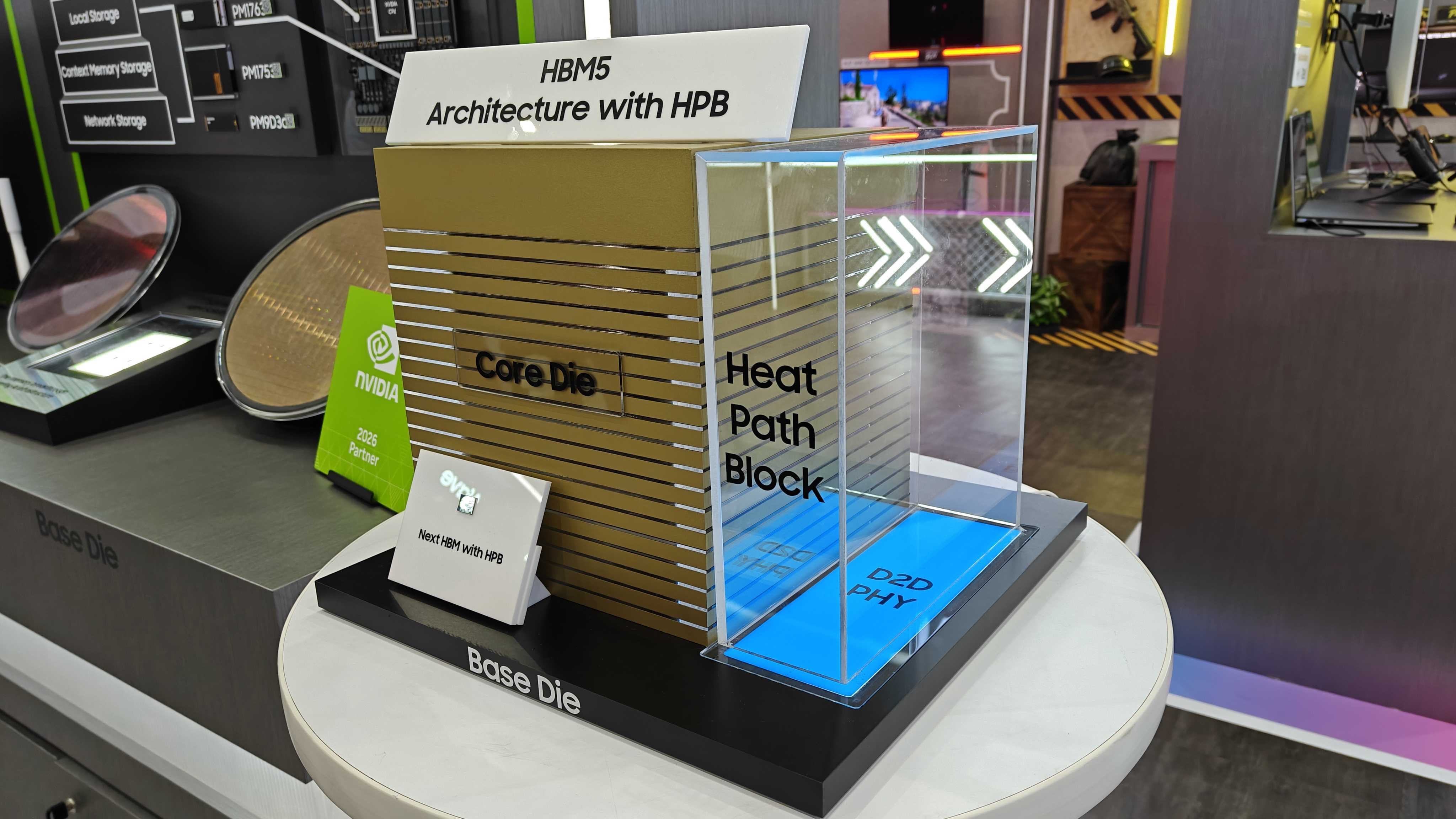
Samsung displayed its first physical mockup of HBM5 memory at Computex 2026 in Taipei. Tom's Hardware dropped by to see its pairing of the eighth-generation AI memory with a new in-package cooling structure it calls Heat Path Block, or HPB. Just last week, rival SK hynix unveiled its own iHBM thermal design, meaning both companies are now focusing on the same heat bottleneck in the die-to-die interface that connects memory to the processor. Samsung also confirmed that it’ll fab HBM5’s base die on its in-house 2nm process, down from the 4nm node used for HBM4 and HBM4E.
Tom's Hardware Premium Roadmaps
Rather than letting heat escape outward through the core dies, HPB builds a separate set of thermal pillars that pull heat from inside the stack and carry it to a spreader sitting above or beside the package, according to Samsung at Computex.
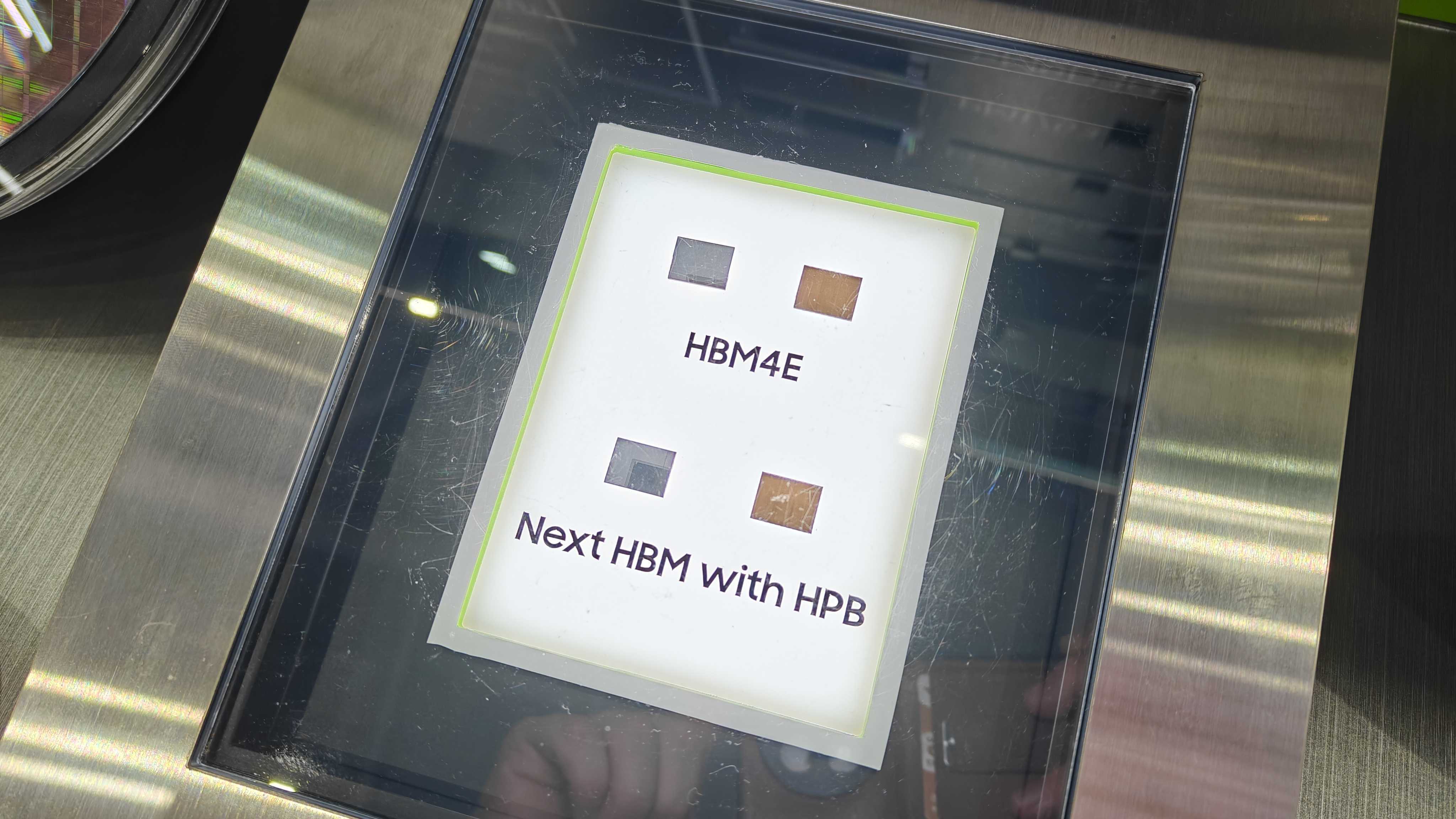
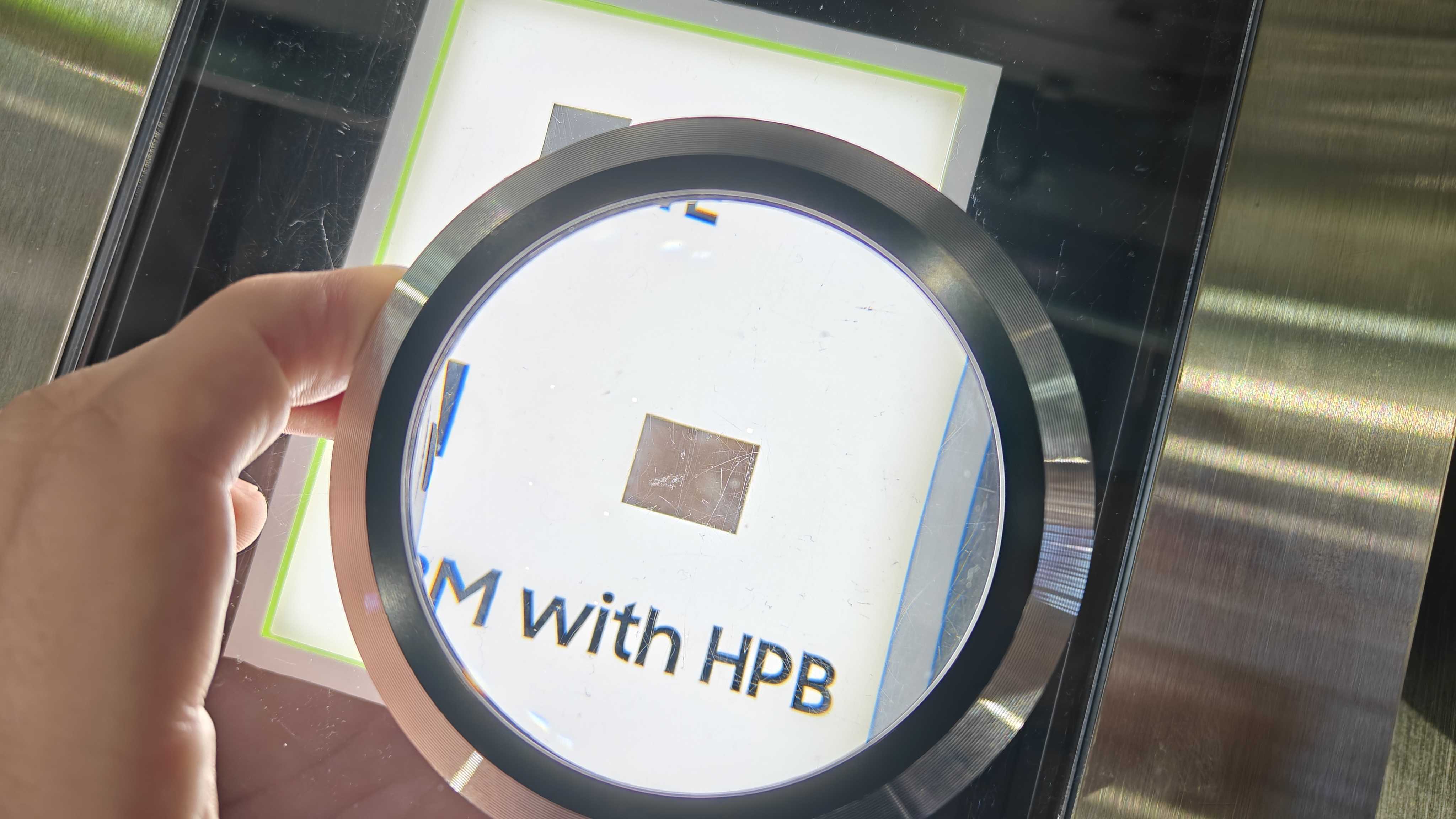
The design concentrates on the D2D PHY layer, the high-speed link between the HBM base die and the GPU, where power density and temperatures increase exponentially as stacks grow taller and run quicker. Samsung said it has already implemented and verified HPB on HBM4E, the generation whose first 12-layer samples it began shipping last month at 14 Gbps, scaling to 16 Gbps, with 3.6 TB/s of bandwidth per stack.
Samsung runs both a memory business and a logic foundry, letting it build the HBM5 stack and the 2nm die beneath it in-house. "AI systems are becoming more powerful and densely integrated, making heat management, data-processing efficiency, and packaging stability just as important as memory performance itself," Song Jai-hyuk, president and CTO of Samsung's Device Solutions division, told reporters at Computex, according to the Korea Herald. Song said the company would keep building its competitiveness in next-generation memory through cooperation with partners, including Nvidia.
Last year, a roadmap from KAIST projected HBM5 reaching a 4,096-bit interface, roughly 4 TB/s per stack, and about 100 watts of per-stack power, a thermal load that goes a long way in explaining why both Korean memory giants are reworking their packaging now rather than at launch.

SK hynix faced the same problem via a different route. Its iHBM design embeds cooling elements made of electrically non-conductive, thermally conductive silicon into the D2D PHY layer, which the company said cuts thermal resistance by more than 30% against current products.
SK hynix has opted to place a cooling element directly at the hotspot, while Samsung has built a route to evacuate heat away from it. Both methods are slated to debut with HBM5, but it’ll be a little while before we see either in action, as neither company expects it to reach mass production before 2028.

Follow Tom's Hardware on Google News, or add us as a preferred source, to get our latest news, analysis, & reviews in your feeds.


 English (US) ·