
 1 month ago
9
1 month ago
9

Samsung Foundry had to delay mass production of chips at its Taylor, Texas fab from the second half of 2024 to sometimes in 2026 due to insufficient yields, reports Business Korea. The publication claims Samsung's yields with SF3 (3nm-class) process technologies that rely on gate-all-around (GAA) transistors are considerably lower than those of its arch-rival TSMC and Samsung is reportedly trying to find the cure for this issue.
Samsung Foundry reportedly went as far as to withdraw personnel from its fab in Taylor, Texas, to cut costs, which could be a part of the company's broader plan reported by Reuters to cut-down its workforce in general. However, Business Korea claims that the company withdrew workforce from the plant due to a delay with its launch to 2026 as it is reconsidering its foundry strategy and refining process technology.
The company's agreement with the U.S. government to receive up to $6.4 billion in grants and loans under the U.S. CHIPS Act is now in jeopardy, as the deal requires the plant to be operational, a condition that is unlikely to be met anytime soon, based on the report.
The Taylor fab was planned as a key facility for producing chips at SF4 (4nm-class) process technologies and below, which in case of the Texas fab timeline includes SF3 (2nd Generation 3nm) and SF3P (which is now called SF2 and formally belongs to 2nm-class nodes). However, due to insufficient yields, particularly with SF2/SF3P process technology, the company has to reassess its plans to concerning production start at the Taylor fab, reports Business Korea. In light of these issues, Samsung has withdrawn most of its workforce from the Taylor plant, leaving only a skeleton crew.
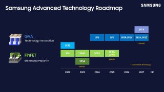
Rumors about insufficient yields at Samsung Foundry have been floating around for years and there are indirect indicators that there are issues with yields particularly at advanced fabrication technologies. Samsung's SF3E (1st Generation 3nm-class node) has only been used for cryptocurrency mining chips, a sign of high defect density that plagues yields of big chips, but its successors SF3 and SF3P have been tapped for a datacenter processor and a smartphone processor.
Yet, reports about Samsung Foundry's yields are often confusing. Even the current Business Korea report claims that Samsung's yields with GAA-based nodes (i.e., 3nm-class and below) are 'around 10% to 50%,' but a few paragraphs earlier the report claims that Samsung's yields at processes of 3nm and below are 'below 50%,' which essentially means that the article contradicts itself. Yet, yields below 50% are insufficient for mass production in most cases, unless chip design has plenty of internal redundancies.
Samsung's chairman Lee Jae-yong, has been proactive in seeking solutions for insufficient yields. Lee has met with key equipment suppliers, such as ASML and Zeiss, in an attempt to address yield and process bottlenecks. However, these efforts have yet to produce significant improvements, which leads to the company's decision to postpone mass production at its state-of-the-art fab in Texas.
Experts point out that Samsung's struggles are not just technical. They highlight deep-rooted internal issues, including a slow decision-making process, excessive bureaucracy, and inadequate compensation, which are believed to be weakening Samsung's competitiveness. Apparently, while the company is eager to spend tens of billions of dollars on production capacity, it does not spend enough on R&D and personnel.


:quality(85):upscale()/2024/10/17/848/n/1922729/9dece426671163b35dcb11.60305022_.jpg)


 English (US) ·