
 8 months ago
104
8 months ago
104
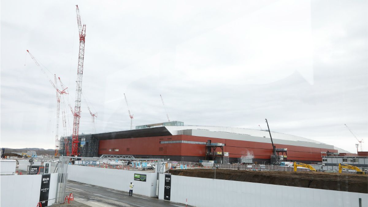
Japan's government-backed chipmaker Rapidus has begun adjusting equipment in order to start test production of wafers later this month. The company, which aims to begin high-volume production on its 2nm-class process technology by 2027, plans to complete the first test wafers by July, according to Bloomberg. After that, the company intends to release process design kits (PDKs) to early customers and offer them an opportunity to prototype their designs.
Rapidus began installing semiconductor production equipment, including ASML's advanced EUV and DUV lithography systems, into its Innovative Integration for Manufacturing (IIM) facility in Chitose, Hokkaido late last year. By now, the company has probably reached the 'first light' on wafer milestone with advanced tools, so it is reasonable to expect it to be able to start pilot production of its own circuits using its 2nm fabrication process that relies on gate-all-around transistors.
One of Rapidus' main advantages over established players like TSMC, Samsung Foundry, and Intel Foundry is projected to be its fully automated advanced packaging capability that will operate at the same fab as the wafer processing, something no company has done yet. This would greatly speed up the production cycle for designs that require advanced packaging. However, for now, Rapidus will only offer pilot production of semiconductor wafers themselves and will not offer test packaging services.
Rapidus is currently setting up a new research and development center, named Rapidus Chiplet Solutions (RCS), at Seiko Epson Corporation's Chitose Plant, located next to the IIM facility. Preparatory work for RCS has been ongoing since October, 2024, and starting in this month, the company will begin installing production equipment at the site, focusing on post-fabrication stages. The facility will be used to build a pilot line aimed at developing scalable manufacturing techniques. Work at RCS will include advancement of redistribution layer (RDL) interposer structures, three-dimensional packaging methods, assembly design kits (ADKs) for complex back-end operations, and known good die (KGD) testing processes.
"The construction of the IIM manufacturing facility at Rapidus has progressed smoothly, and by the end of last fiscal year we had completed the installation of the semiconductor manufacturing equipment necessary for the start of pilot operations," said Dr. Atsuyoshi Koike, representative director and CEO of Rapidus. […] "With the approval of the NEDO project plan and budget, we will start up the pilot line in April, which will steadily lead to the start of mass production targeted for 2027."


 English (US) ·