
 5 months ago
87
5 months ago
87
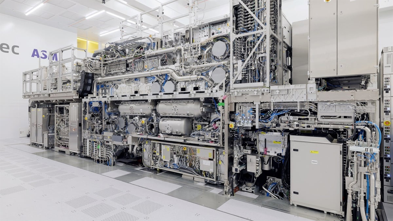
Creating a powerful, reliable, and manufacturable light source for modern chipmaking lithography tools is one of the most complex challenges in today's industry. Among all makers of litho systems, only ASML has successfully created EUV light to print the smallest chip features, but a startup has a radical new idea to change the status quo.
However, Immersion Semiconductor, a San Francisco-based startup backed by venture capital firm Y Combinator, has plans to develop a light source based on a compact particle accelerator, which it claims would be 33 times more powerful than ASML's existing technology and could pave the way for producing finer chip features.
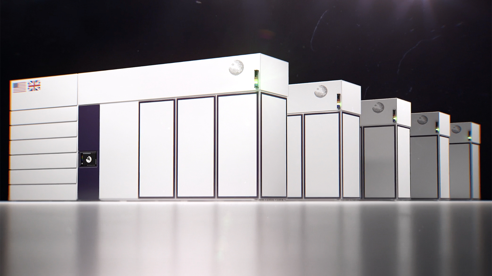
At the heart of Inversion Semiconductor's technology is a 'tabletop' particle accelerator that is 1000x smaller than traditional particle accelerators and yet can deliver output power of up to 10 kW. Despite its tiny dimensions, Inversion claims that its light source, leveraging the laser wakefield acceleration (LWFA) method, can either speed up chipmaking by 15 times (assuming one 10 kW light source powers one lithography system) or power multiple chipmaking tools simultaneously, thereby cutting costs.
However, there are major challenges for the budding startup, as this specific type of accelerator requires petawatt-class lasers, which are both costly and power hungry. Additionally, unless Inversion Semiconductor collaborates with ASML (or perhaps other manufacturers of lithography machines), it would need to develop its own lithography systems and create a new ecosystem for its scanners, which is a time-consuming and expensive endeavor.
Given that Inversion Semiconductor has no experience with building high-volume production 24/7 fab tools, the company's ambitions are lofty, and there's no guarantee it will fulfill the promise it's making on paper.
10 times more power-hungry than ASML
Inversion Semiconductor was founded in 2024 by Rohan Karthik (CEO) and Daniel Vega (CTO), both of whom hold master's degrees in mechanical engineering and applied physics. The company is backed by Y Combinator. Inversion Semiconductor's goal is to develop a compact, high-performance light source based on a particle accelerator that would offer an output power of 10 kW, which is 10 times more powerful than what ASML plans to achieve over the next decade.
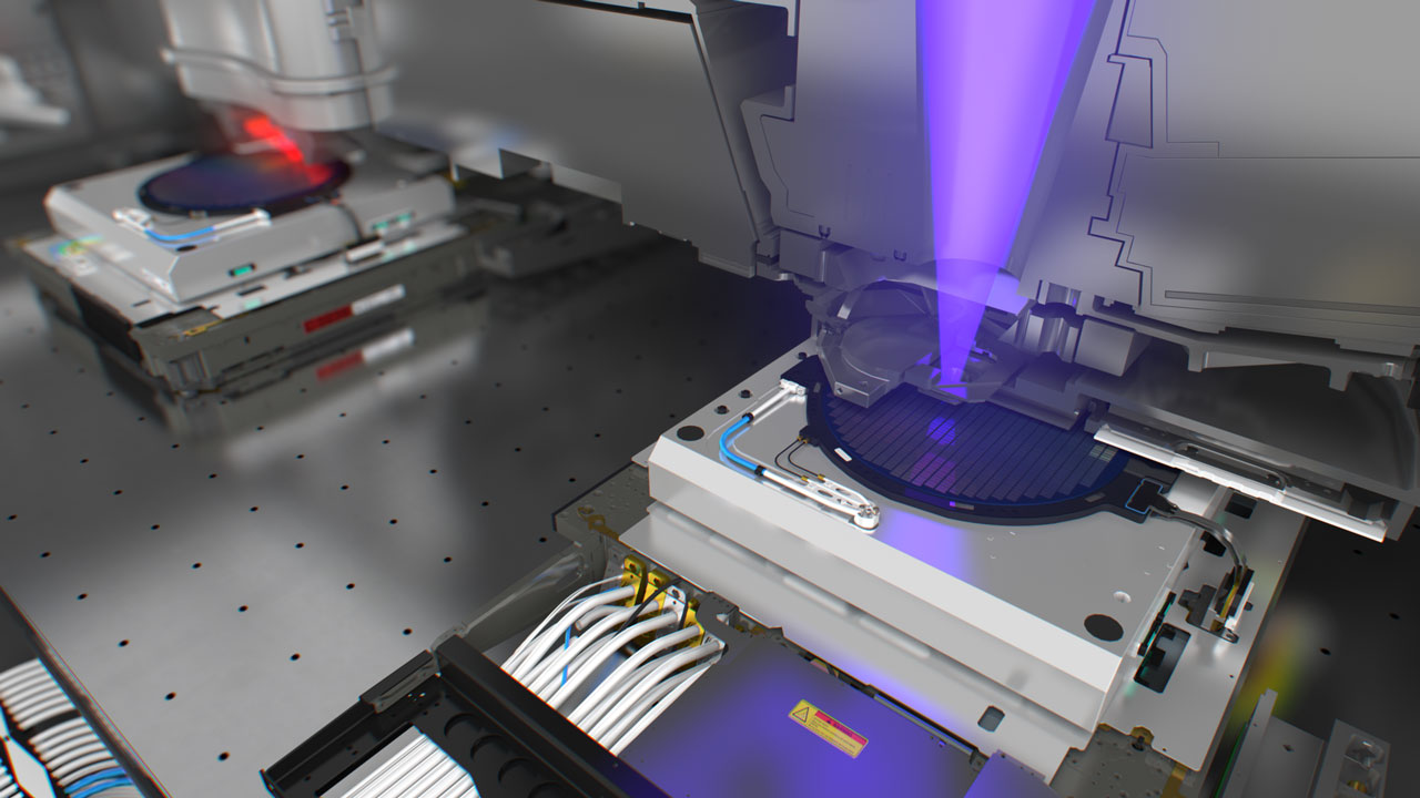
This particle accelerator could produce lasers with wavelengths between 20nm and 6.7nm, including 13.5nm light used by ASML for both Low-NA EUV and High-NA EUV lithography tools today.
Light with a sub-10nm wavelength is called a soft X-ray, which is not currently used for chip production due to its high absorption rates by most materials. So, while sub-10nm wavelengths are not currently used in chip production, it might prove to be a promising field for research in the long-term future.
Inversion's ambitions do not end with the development of just a light source, but span all the way to building complete lithography tools to compete against ASML directly.
Using particle accelerators as light sources for lithography tools is a widely discussed and researched topic in the industry, but Inversion Semiconductor plans to use what it calls 'tabletop particle accelerators' that can accelerate electrons to extremely high energies over centimeters, rather than kilometers, as seen in accelerators such as the Large Hadron Collider used by CERN.
Riding on the wakefield waves
Immersion intends to use accelerators relying on the laser wakefield acceleration (LWFA) technique, which is significantly different compared to methods used by ASML and CERN. LWFA uses powerful, ultra-short (femtosecond-scale) laser pulses interacting with plasma, consisting of free electrons and positively charged ions.
When an intense laser pulse travels through plasma, it creates strong electric fields by pushing electrons aside and generating plasma waves, or 'wakefields' behind it. Electrons can become trapped and accelerated rapidly within these waves, gaining substantial energy in a very short distance as they rush back to their original position. The plasma wave accelerates electrons in fields that are 100 – 1000 times stronger than those found in a conventional accelerator, according to the Imperial College London.
The accelerated electrons can then be used for various practical applications, including compact X-ray sources and semiconductor lithography, just to name a few. Unlike traditional EUV sources, the LWFA method generates radiation that is coherent, monochromatic, and precisely tuneable, enabling wavelengths shorter than 13.5 nm (e.g., 6.7 nm target, which is far from industrial deployment), which could be instrumental for next-generation lithography systems.
The LWFA mechanism accelerates electrons to energies reaching multiple giga-electron volts (GeV) over distances as short as a few centimeters, thus miniaturizing high-energy electron acceleration systems dramatically, from large facilities down to tabletop-sized devices, which could spark further innovation for the semiconductor industry.
Immersion Semiconductor's progress to date includes setting up a small laser laboratory within the Y Combinator offices to develop new laser stabilization techniques, and building initial LWFA prototypes capable of producing short-wavelength radiation. They have also partnered with the Lawrence Berkeley National Laboratory and the BELLA Center to collaborate on the BELLA-LUX project, focusing on refining laser stability and improving the generation of suitable light for semiconductor use.
The company's immediate goal is to develop Starlight: a high-power, tunable light source capable of producing 1 kW of soft X-ray light in the 20 nm to 6 nm wavelength range. If successful, the device could find use in applications like industrial X-ray imaging and semiconductor mask inspection. Companies such as Tesla and Applied Materials have expressed interest in these early-stage developments, according to Immersion Semiconductor.
In parallel, the company is working on advanced mirror systems to reflect and focus the generated EUV light (i.e. higher than 10nm), which are necessary to direct the light precisely for wafer patterning. The first lithography system based on this technology — designated LITH-0 — will be powered by Starlight, with the goal of demonstrating practical silicon wafer patterning capabilities. However, no-one knows when Inversion Semiconductor's LITH-0 will be complete, and fully-functional.
Are there any Caveats? Many!
On paper, Inversion Lithography's plans seem sound and the LWFA method of generating EUV radiation (or light) seems almost perfect. However, there are many caveats.
First up, an LWFA accelerator chamber may be small, but it requires a petawatt-class, ultrafast laser systems which are extremely complex, large, and expensive. Cooling and maintaining such lasers for reliable, non-stop fab operation is something that nobody has tried. It is also unclear whether Immersion Semiconductor's setup can fire those lasers at a consistent repetition rate per second.
Secondly, even researchers from the John Adams Institute for Accelerator Science at Imperial College London admit that LWFA produces electron beams with large energy spread (variation in electron energies) and beam divergence (wider spread of trajectories) at beyond 1 GeV.
For lithography, the generated light must be highly stable in wavelength, direction, and coherence to achieve precise and repeatable patterning. Instability translates into poor resolution leading to performance variability and yield loss.
Thirdly, while today LWFA-based tools featuring a laser with 13.5nm light source can use mirrors and optics developed for ASML's Low-NA and High-NA EUV tools, should they move to shorter wavelengths, they are poised to use new mirrors and optics. This will be a problem, of course, if Inversion Lithography actually decides to develop its own lithography systems, but, this means it will have to develop a whole new ecosystem.
A more realistic variant could be making its LWFA-based source compatible with existing tools from ASML. However, there is a problem too. Integrating an LWFA light source with existing EUV lithography scanners would be complex as it would require developing new beam shaping, focusing, and metrology systems, just to name a few challenges. While ASML has solved all the challenges associated with its Cymer light sources, we can only wonder whether the company is interested in making its tools work with a third-party tool. As for other makers of litho machines — Canon and Nikon — they have not managed to go beyond KrF and ArF lasers and tools, respectively, so chances that they will manage to build EUV (or beyond EUV) scanners are low. Also, keeping in mind that we are talking about an at least 1 kW light source, the industry will also need new resists, pellicles, and other expendables to make everything work.
Perhaps the biggest challenge for Inversion Lithography is that it does not have any experience in production of rapidly-serviceable mass-produced tools that are engineered for fabs operating 24/7 and are highly compatible with other production equipment in the building.
Summary
Inversion Lithography aims to develop a compact, LWFA-based light source that 10 times more powerful than ASML's current EUV light sources while also targeting even shorter wavelenghts. Inversion says that its light sources will be tunable and will create coherent radiation for finer semiconductor patterning. Eventually the company aims to build a light source with a 10 kW performance (10 times more powerful compared to what ASML plans over the next decade), it can either greatly speed up production of chips (by 15 times, the company claims), or power multiple lithography systems with one light source, thus cutting down costs.
However, there are major challenges as an LWFA-based accelerator require a petawatt-class laser, which consumes a lot of power and is expensive. Also, unless Inversion teams up with ASML (an unlikely scenario) or other makers of litho tools like Canon and Nikon (also unlikely) and develops its own scanners, it will have to develop an all-new ecosystem for its machines, which is timely and extremely costly. Also, if the company goes down this path, it will have to gain experience in creating and maintaining high-volume production 24/7 fab tools.
Follow Tom's Hardware on Google News to get our up-to-date news, analysis, and reviews in your feeds. Make sure to click the Follow button.


 English (US) ·