
 2 hours ago
11
2 hours ago
11

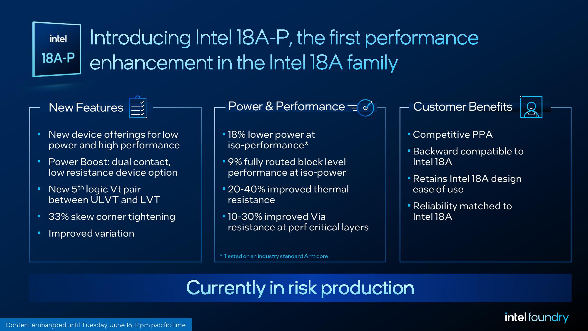
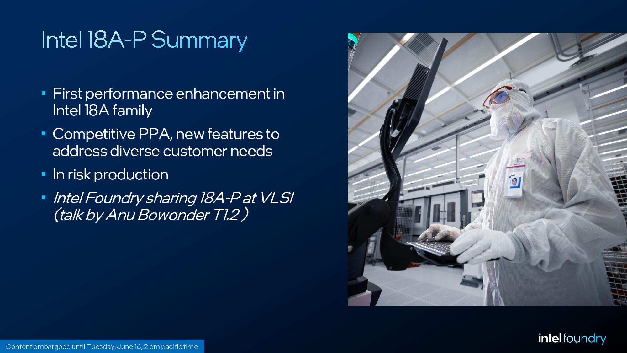
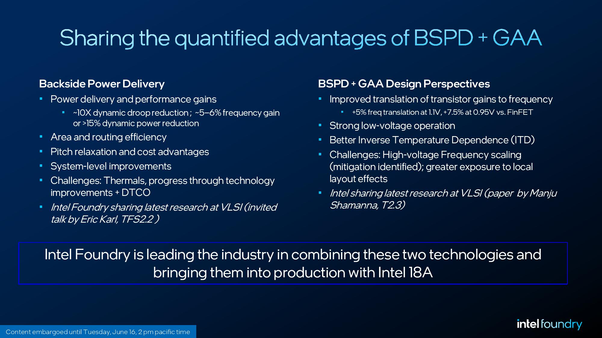
Following a paper published earlier this year, Intel has provided more details on its optimized 18A-P process at VLSI 2026. The performance-optimized node is an enhancement of 18A that Intel is using in products like Panther Lake and Xeon 6+, promising a 9% improvement in performance at the same power, or an 18% reduction in power consumption at the same performance level. In addition to greater technical detail, Intel has revealed that 18A-P has entered risk production.
Go deeper with TH Premium: Chipmaking
If you’re unfamiliar with that term, it’s the stage of semiconductor manufacturing just before high-volume mass production. It’s a low-volume manufacturing stage where Intel will produce full wafers of 18A-P on a standard production line, just with a limited scope to gather data on defect rate, performance, and variability before full production begins. Risk production usually leads mass production on advanced logic by 12 to 24 months, though we’re not dealing with an entirely new node here, so expect a tighter timeline.
18A-P is a revision of 18A, and although it carries new transistor designs (more on those soon), they live in the same libraries at cell heights of 180mm (High Performance) and 160mm (High Density). The new process is backward compatible with 18A designs, meaning designers can port to 18A-P without making any changes. Some of the new transistor options could spur a design change, but it’s not required; anything built on 18A can be built on 18A-P with more minor performance benefits, but no design changes.
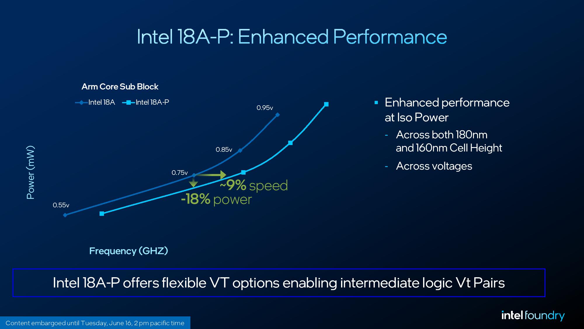
For performance, Intel arrived at its numbers by testing on a standard Arm core subblock, noting the 9% frequency increase or 18% reduction in power specifically at 0.75 volts. The chart you can see in the gallery below is a beautified version of a chart published in Intel’s original research; in other words, it’s not just random lines without any correlation. You can see that even as voltage moves outside that 0.75V mark, 18A-P retains a frequency/power improvement.
With 18A-P, Intel is adding three transistor designs to its library. The W1 design is available in the 180mm cell height library (it was previously available in the 160mm library), while W1.5 is available in the 160mm library. The enhanced W3P design is available in both libraries. W1 and W1.5 are both narrow designs optimized for low-power usage, helping fill gaps in power-optimized designs in Intel’s library, while W3P is a new dual-contact transistor with “Power Boost,” as Intel calls it. As you can see in the gallery below, the original W2 and W3 designs still see a boost in ring oscillator frequency (moving an electrical signal through a ring of inverters) with 18A-P.

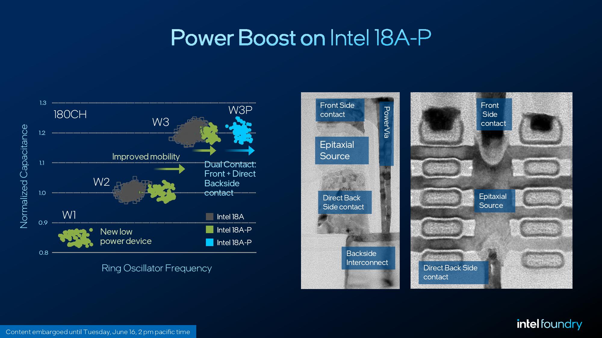
W3P is the most interesting design due to Power Boost. 18A already uses backside power delivery with PowerVia, which uses the back of the wafer to route power, freeing up space for front side signal wiring and reducing thermal resistance. The W3P design has contacts on the front side and backside, reducing parasitic resistance and enabling higher drive current to speed up switching.
Although the standard W2 and W3 transistors will see a benefit moving from 18A to 18A-P, it’s minor. The biggest frequency improvement comes from W3P, while W1 pushes 18A-P down to lower capacitance levels for energy-optimized designs.
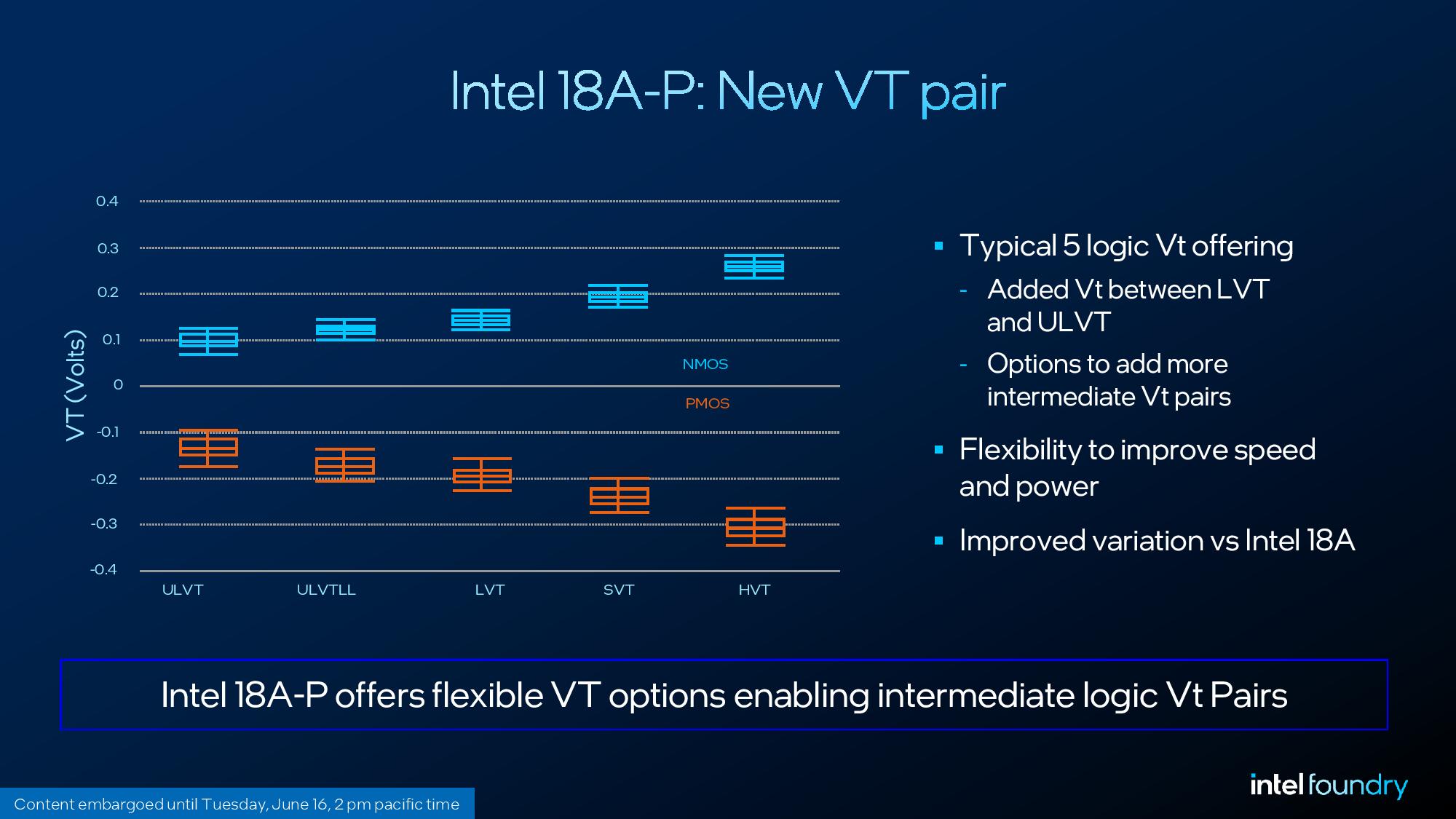
Intel is also adding a new VT (threshold voltage) pair to its lineup. Typically, we see four flavors of VT pairs: HVT, SVT, LVT, and ULVT, noting high, standard, low, and ultra-low threshold voltage, respectively. The lower the threshold voltage, the less power a transistor needs to activate, and therefore the more power it leaks. So, ULVT transistors are the most performant, but they leak the most power, while HVT transistors are the least performant but leak the least amount of power. Chip designers need to balance these different flavors of threshold voltage for their application.
The new VT pair adds another option: ULVTLL, or Ultra-Low Voltage Threshold Low Leakage. It lives between ULVT and LVT, offering better performance than LVT but lower leakage than ULVT. Like the new transistor design, it gives designers more flexibility when designing a chip for 18A-P.
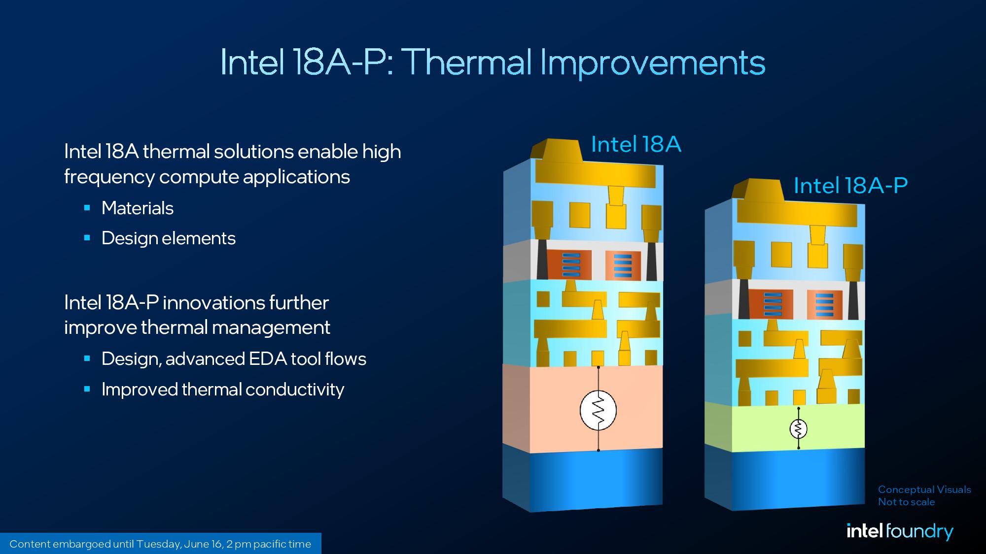
In addition to the expanding 18A-P’s capabilities, Intel says the revision comes with a 20% to 40% improvement in thermal resistance, as well as a 10% to 30% improvement in via resistance at “perf critical layers.” The reduction in thermal resistance comes from grinding the wafer down with advanced EDA tools for better thermal conductivity.
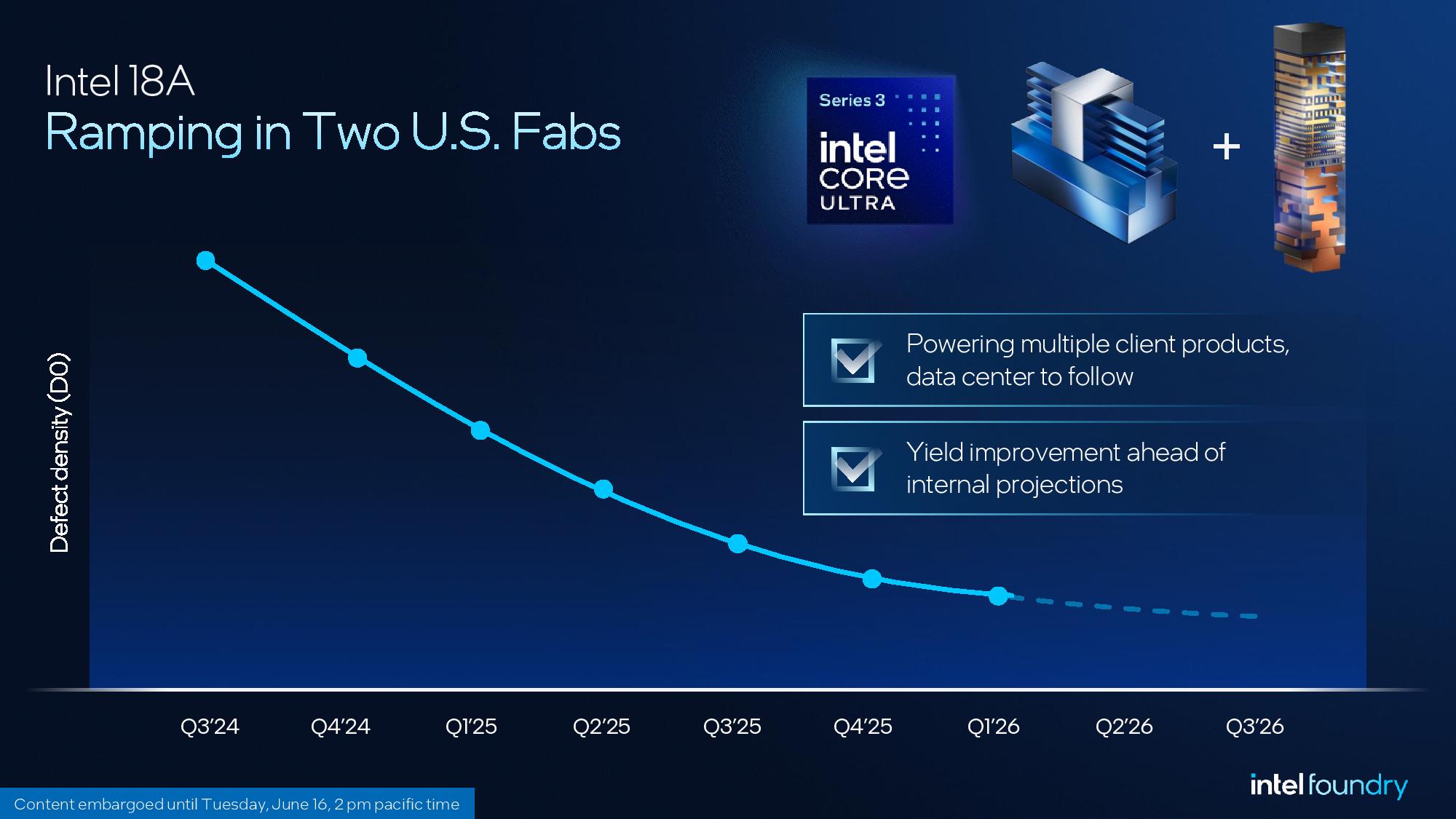
Intel 18A is currently ramping in two U.S. fabs, and although the company has taken some heat for poor 18A yields, Intel says that defect rates continue to drop along with its expectations. 18A is being used already in Panther Lake and Xeon 6+, and Intel is reportedly in talks with Apple and Nvidia to build on 18A, as well.
Full presentation


Follow Tom's Hardware on Google News, or add us as a preferred source, to get our latest news, analysis, & reviews in your feeds.


 English (US) ·