
 3 weeks ago
26
3 weeks ago
26
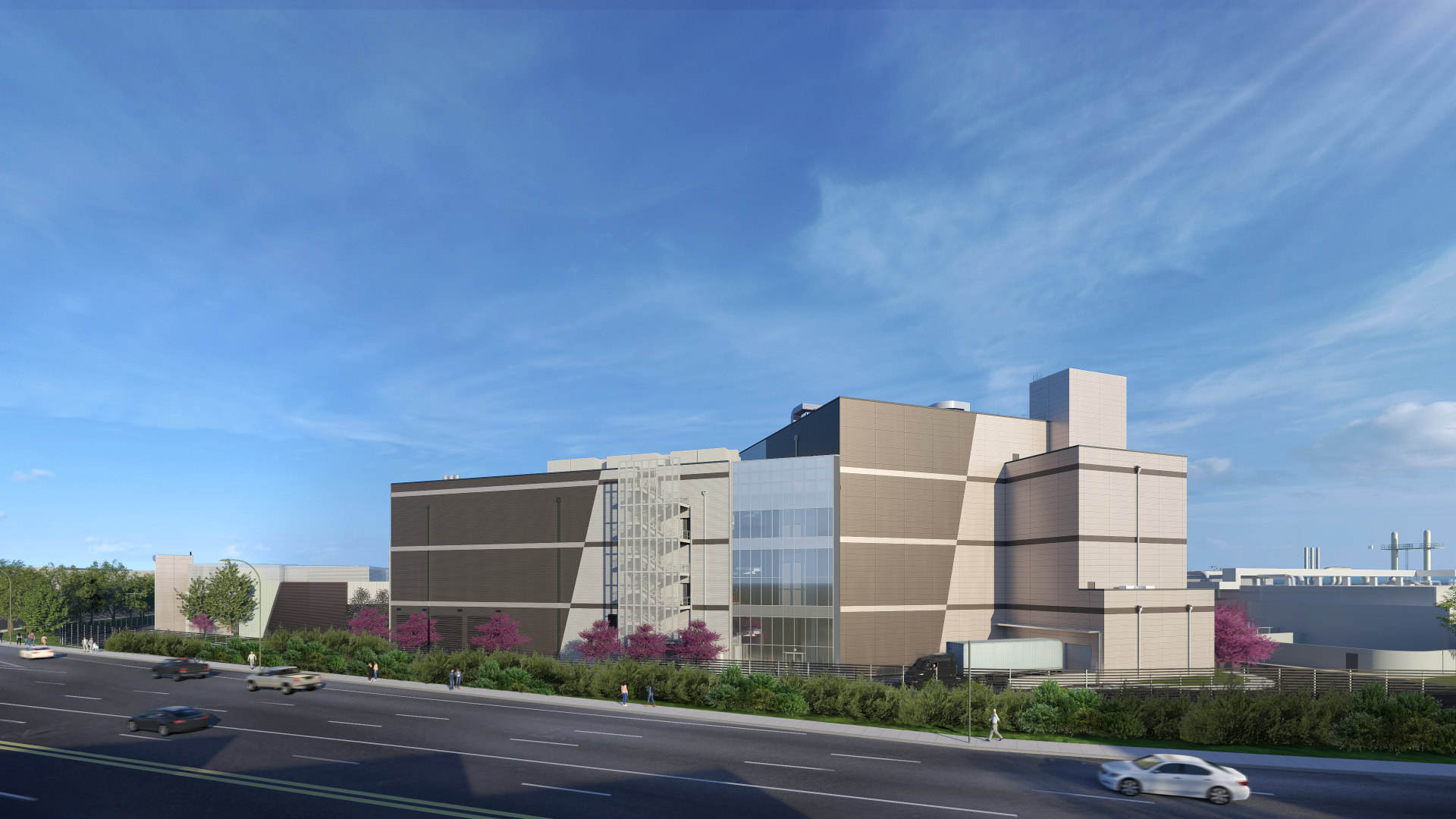
Intel this week initiated expansion of its Bowers Campus in Santa Clara, California, in a bid to produce more photomasks (reticles) in the U.S. The company intends to build a new manufacturing facility and a new utility building at the site, which will reinforce the site's position as a key producer of photomasks for Intel.
Go deeper with TH Premium: Chipmaking
Earlier this year Intel obtained approval to build a new 107,000 square feet (9,940 square meters) manufacturing facility with Class 1 cleanroom at its Bowers Campus, and this week it formally began construction on the expansion, which it kicked off at a ceremony attended by its top executives and Santa Clara mayor Lisa Gilmor. The new facility will be able to write 6-inch × 6-inch photomasks both for DUV and EUV layers and a variety of nodes (from 32nm down 1.4nm-class), though the primary focus of the facility is to produce reticles for leading-edge process technologies — such as Intel's 18A, 18A-P, 14A, and more advanced — that rely on advanced DUV, EUV and eventually High-NA EUV tools and require more advanced photomasks, such as those that feature extremely dense patterns and use curvilinear optical proximity correction (OPC) with curved geometric shape.
Intel is one of a few leading chipmakers in the world that still maintains a world-class mask writing shop — which is important, as every advanced product requires hundreds of masks, and every mask revision directly affects production schedules. In addition, producing masks in-house is getting particularly important when it comes to reticles for EUV layers as EUV tools tend to damage masks over time (despite usage of protective pellicles), so having the ability to make new masks in a short amount of time is crucial.
Furthermore, Intel is the only semiconductor producer to make its own tools for photomasks writing at its IMS Nanofabrication subsidiary. Historically, reticles were patterned using a single e-beam tool, which was slow. By contrast, IMS produces multi-beam mask writers (MBMWs) that project 262,144 independently programmable electron beams simultaneously, which increases throughput by orders of magnitude at a nanometer-scale placement accuracy.
"Santa Clara has been home to some of Intel's most important manufacturing innovations for decades," said Dr. Frank Abboud, VP Intel Foundry & GM of Intel Mask Operations. "By expanding the Bowers campus mask operations, we're strengthening a critical capability that supports advanced process technology production around the world and reinforces Intel Foundry's commitment to advancing U.S. semiconductor manufacturing leadership."
Intel's Bowers Campus in Santa Clara has been dedicated to mask production since 1986. The site forms the company's primary mask manufacturing infrastructure supporting together with the company's facility in Hillsboro, Oregon. Production of non-critical masks has historically been outsourced, though we do not know whether the company still does that.

Follow Tom's Hardware on Google News, or add us as a preferred source, to get our latest news, analysis, & reviews in your feeds.


 English (US) ·