Intel has published a paper about its 18A (1.8nm-class) fabrication process at the VLSI 2025 symposium, consolidating all its information about the manufacturing technology into a single document. The new 18A production node is expected to deliver significant improvements in power, performance, and area over its predecessor, increasing density by 30% while enhancing performance by 25% or reducing power consumption by 36%.
But, perhaps more importantly, 18A will be Intel's first process technology in years that will compete head-to-head with TSMC's leading-edge technology when both enter mass production in the second half of this year.
PPA advantages
Intel's 18A process node is designed for a wide range of range of products across both client and datacenter applications, and the first Intel's product to use it will be the Panther Lake CPU, which is due to be formally announced later this year. To address different applications, Intel 18A has two libraries: high-performance (HP) with 180nm cell height (180CH) and high-density (HD) with 160nm cell height (160CH) for lower-power applications.
Swipe to scroll horizontally
| Row 0 - Cell 0 | Intel 3 vs Intel 4 | 18A vs Intel 3 |
Power | ? | 36% (at 1.1V) - 38% (at 0.75V) |
Performance | 18% (?) | 18% (at 0.75V) - 25% (1.1V) |
Density | - | 1.3X |
SRAM Cell Size | 0.024 µm² | 0.021 µm² |
Transistor | FinFET | RibbonFET GAA |
Power Delivery | Front-side | PowerVia BSPDN |
HVM | mid-2024 | H2 2025 |
Intel says that compared to Intel 3, its 18A fabrication technology boosts performance by 25%. It manages to achieve this without increasing voltage or circuit complexity when running a typical Arm core sub-block, implemented using a 180CH HD library at 1.1. When operating at the same clocks and 1.1V voltage, it also cuts power usage by 36% compared to the same design on Intel 3. At a reduced voltage of 0.75V, 18A offers an 18% speed increase and uses 38% less energy. Furthermore, designs fabricated on 18A occupy roughly 28% less area than those built with Intel 3.
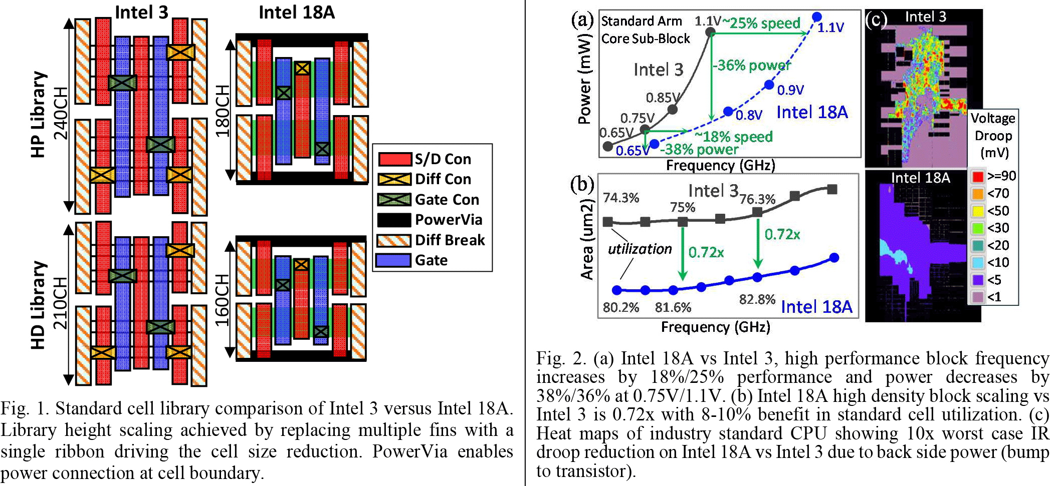
There is a major catch about comparison of voltages between Intel 3 and 18A. The former supports <0.6V, 0.75V, 1.1V, and 1.3V, which makes it particularly suitable for data center devices. This type of workload needs to burst to high clocks, across dozens of cores when demanding peak performance. Then, it'll need to throttle down to a low-power state to save power. To contrast, 18A seems to support 0.4V, 0.75V, and 1.1V, which very good for client PCs and data center CPUs, but may not be ideal for processors that need maximum clock speeds. However, other advantages of Intel's 18A will likely offset the lack of 1.3V support for the vast majority of applications (more on this later).
As for SRAM, Intel's 18A process includes a high-density SRAM bit cell measuring 0.021 µm², translating to an SRAM density of roughly 31.8 Mb/mm². This is a major improvement over the 0.024 µm² bit cell used in Intel 4. This puts Intel 18A on par with TSMC's N5 and N3E nodes in terms of SRAM density. However, TSMC’s upcoming N2 process goes further, reducing the bit cell to approximately 0.0175 µm² and achieving a higher density of around 38 Mb/mm².
Swipe to scroll horizontally
Tom's Hardware | Intel 7 | Intel 4 | Intel 3 | Intel 18A |
Contacted Poly Pitch | 54nm/60nm | 50 nm | 50 nm | 50 nm |
Fin Pitch | 34 nm | 30 nm | 30 nm | ? |
M0 Pitch | 40 nm | 30 nm | 30 nm | 32 nm |
High Performance Library Height | 408 nm | 240 nm | 240 nm | 180 nm |
High Density Library Height | - | - | 210 nm | 160 nm |
HP Library Height x CPP | 24.4K nm² | 12K nm² | 12K nm² | 9K nm² |
HD Library Height x CPP | - | - | 10.5K nm² | 8K nm² |
Intel's 18A relies on the company's 2nd generation RibbonFET gate-all-around (GAA) transistors, and a PowerVia backside power delivery network (BSPDN). We investigate exactly how Intel managed to implement GAA transistors and BSPSN below.
RibbonFET
In GAA transistors, the gate completely wraps around the channel, offering superior electrostatic control compared to FinFETs, which only wrap around on three sides. Such an architecture enables engineers to finely tune device characteristics for either high performance or low power consumption by adjusting the total effective channel width (Weff). This is typically achieved by varying the width and number of stacked nanosheets. More sheets, alongside wider sheets, can increase drive current and performance at the cost of power, while fewer or narrower sheets reduce both performance and power consumption.
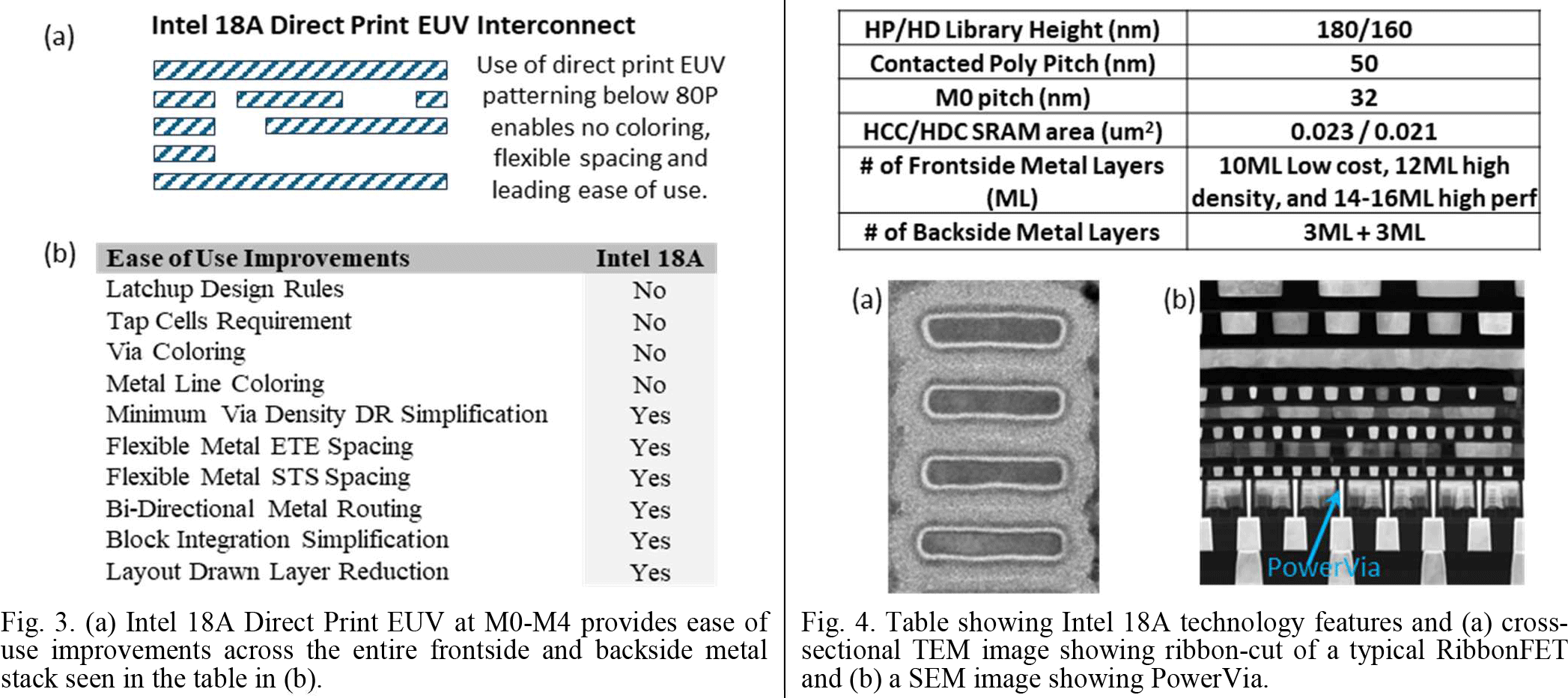
Intel's 18A RibbonFET transistors feature four nanoribbons and support eight distinct logic threshold voltages (VTs) — four for NMOS, and four for PMOS — spanning a 180mV range. This level of VT granularity is achieved through dipole-based work-function tuning, a method that allows precise control of transistor behavior without altering its physical dimensions. This approach is especially important, given the tight spatial constraints in GAA transistor structures, such as RibbonFETs, where traditional methods, like doping adjustments, are limited.
An Intel graph from the paper shows that despite this wide VT range, the transistors exhibit strong electrical characteristics, including steep subthreshold slopes and well-behaved drive currents across both Id–Vg and Id–Vd curves. These results confirm that Intel has successfully maintained device performance and control across the entire VT spectrum, which enables flexible circuit design choices that balance frequency, power, and leakage within the same process.
PowerVia
Intel's PowerVia backside power delivery network (BSPDN) relocates power delivery from the top metal layers to the rear side of the chip, creating a physical separation between power and signal wiring. This technique addresses issues like rising resistance in the vertical connections of in the back-end-of-line (BEOL) layers, which in turn enhances transistor efficiency and reduces power usage. Additionally, it prevents signal degradation caused by power interference and allows for tighter packing of logic elements, increasing overall circuit density.
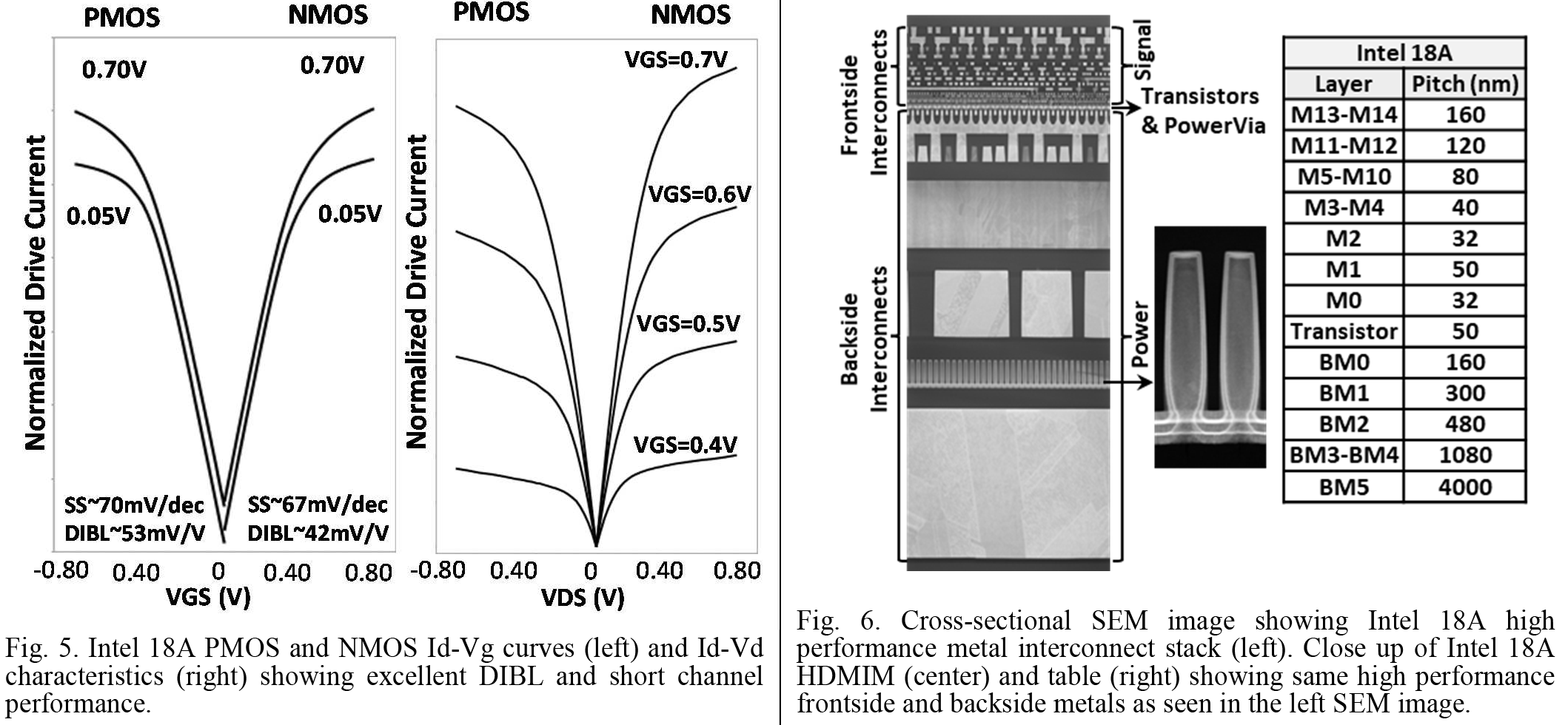
Intel's PowerVia delivers power to transistor contacts, which is a slightly less sophisticated approach compared to TSMC's Super Power Rail (coming in 2H 2026 along with A16), which connects directly to each transistor's source and drain. In addition to BSPDN, Intel also implemented its new high-density metal-insulator-metal (MIM) capacitor to enhance power supply stability.
Intel has now disclosed the key benefits of its backside power routing. First up, PowerVia increases transistor density by 8% to 10%, which is quite a sizeable part of 18A's overall 1.3X transistor density increase over Intel 3. Secondly, the front-side metal layers in its 18A process achieve approximately 12% better resistance-capacitance (RC) performance and show a 24% to 49% decrease in via resistance compared to Intel 3, thanks to improved metallization techniques and the use of ultra-low-k dielectrics. Thirdly, 18A's PowerVia reduces voltage droop compared to Intel 3 (the worst-case scenario for Intel 3) by up to 10 times. Lastly, BSPDN simplifies chip design as it simplifies the routing of signal and power wires.
PowerVia's reliability
Since PowerVia is the industry's first backside power delivery network (BSPDN) used in mass production, Intel also presented reliability test results. These demonstrate its long-term durability and chip-package interaction (CPI) performance.
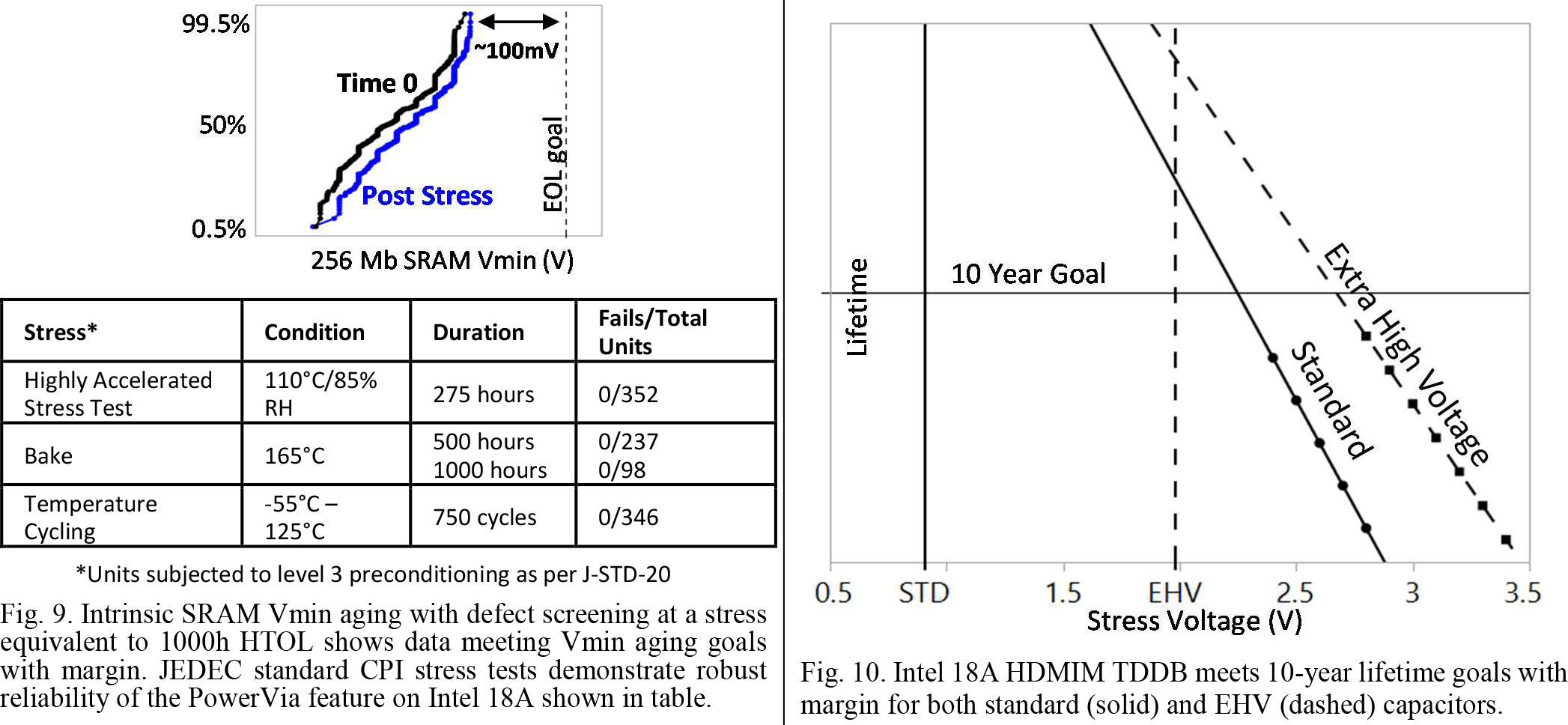
According to JEDEC-standard TQV tests, PowerVia passed multiple stress conditions with zero failures, including highly accelerated stress testing at 110°C and 85% humidity for 275 hours, extended high-temperature bake tests up to 1000 hours at 165°C, and 750 cycles of temperature swings from –55°C to 125°C. These results confirm that PowerVia can withstand harsh operating environments, without compromising structural or electrical integrity.
In addition to CPI reliability, Intel evaluated the impact of PowerVia on SRAM aging and performance stability. Under conditions equivalent to 1000 hours of high-temperature operation, SRAM arrays maintained stable minimum operating voltage (Vmin) with margin, showing no signs of degradation. This suggests that PowerVia does not negatively affect sensitive on-chip memory and is robust enough to support both digital logic and embedded SRAM under extended stress. Together, these findings are meant to affirm PowerVia's readiness for deployment in high-performance, long-lifecycle computing platforms.
Manufacturability
In addition to improving performance, reducing power consumption, and enabling higher transistor density, Intel's 18A simplifies production flows and simplifies chip design.
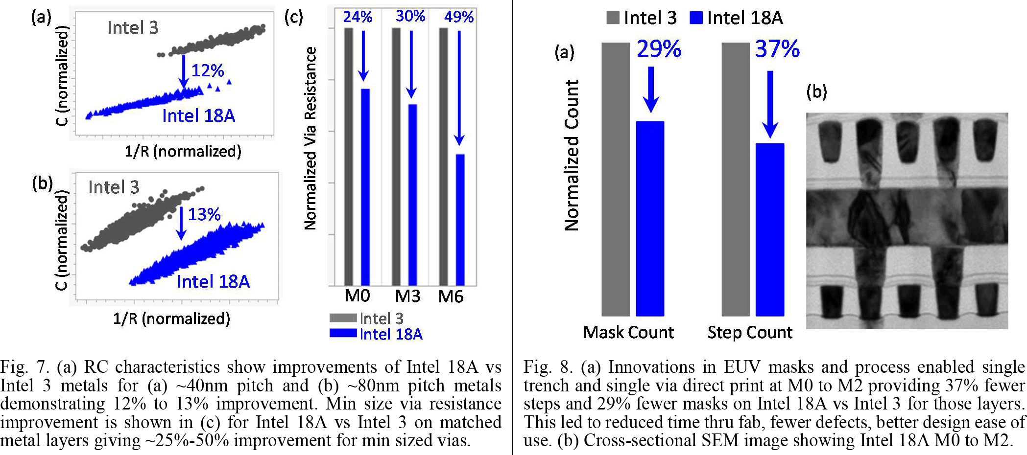
By moving power delivery to the backside, Intel eliminates the need for a front-side power grid, which, combined with direct EUV patterning, lowers the total number of masks and simplifies the front-end metal process. By using low-n absorber reticles with tailored dimensional adjustments, Intel also enabled single-pass EUV patterning for the M0–M2 metal layers. This simplification of the lower metal layers reduces process complexity and helps offset the cost of adding extra backside metal layers, which are based on mature, low-cost fabrication techniques. As a result, the overall design process becomes easier and cheaper.
In addition, the backside metal layers of 18A's PowerVia are designed for low resistance and high thermal conductivity, which helps manage the increased power density from the GAA transistors. Also, carrier wafer bonding is optimized for heat removal through the backside, addressing the thermal challenges introduced by high-performance transistors. Finally, PowerVia is compatible with advanced packaging methods like Foveros and EMIB, though we already know this from the fact that Panther Lake uses 18A tiles as well as Foveros 3D.
Summary
Intel's comprehensive technical overview of its 18A process node has highlighted the architecture, performance, and manufacturability improvements that position it as a competitor to TSMC's upcoming N2. The 18A process introduces Intel's second-generation RibbonFET (GAA) transistors and the industry's first mass-production-ready backside power delivery network, PowerVia.
Together, these innovations enable up to 25% higher performance or 36% lower power consumption compared to Intel 3, while also increasing transistor density by about 30%.
Intel's PowerVia contributes an 8–10% density gain, 12% RC improvement in metal layers, and up to 10 times lower voltage droop.
The new node has also passed stringent JEDEC reliability tests, including 1000-hour high-temperature aging and extensive thermal cycling to verify that it can be used for designs meant to work for a long time. Additionally, Intel further streamlined front-end patterning using single-pass EUV at M0–M2, thereby reducing mask counts and simplifying the design.
However, whether or not 18A can help Intel restore some of the lustre to its brand remains to be seen, as the company continues to wade its way through rocky waters.
Follow Tom's Hardware on Google News to get our up-to-date news, analysis, and reviews in your feeds. Make sure to click the Follow button.

 5 months ago
122


 English (US) ·