
 3 weeks ago
62
3 weeks ago
62
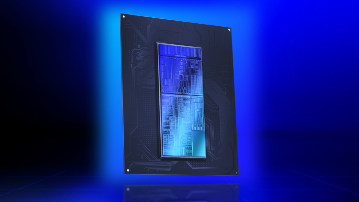
Intel has entered high-volume manufacturing using ASML's High NA extreme ultraviolet (EUV) lithography technology for a subset of its Intel Core Ultra Series 3 "Panther Lake" processors, becoming the first company to ship high-volume logic products manufactured with the technology. ASML announced the milestone in an official press release on Wednesday, July 15, confirming that Intel Foundry is running the qualified High NA layers on its Intel 18A process node in Oregon.
Go deeper with TH Premium: Chipmaking
According to ASML, Intel is using High NA EUV to pattern selected Intel 18A layers, with products already shipping to customers at yields matched to those achieved on ASML's existing NXE EUV platform. These layers are dual-qualified, meaning the same layer can be exposed on either an existing 0.33 NA NXE scanner or a 0.55 NA EXE scanner, with the resulting wafers being interchangeable.
High NA EUV has long been viewed as the successor to today's EUV lithography, promising to extend semiconductor scaling by enabling manufacturers to print smaller, denser circuit patterns that are becoming difficult to achieve with existing tools. Until now, the platform had been confined to R&D work. ASML’s announcement marks the first time High NA EUV has been used to produce and ship a high-volume commercial logic product.
Panther Lake, built on the Intel 18A manufacturing process, is spearheading this transition. Rather than replacing the company's entire lithography flow, Intel is applying High NA EUV to specific layers while the remainder of the chip continues to be manufactured using conventional lithography.
High NA EUV builds on the same 13.5-nanometer extreme ultraviolet light used by today's scanners but increases the optical system's numerical aperture (NA) — how much light a lens system can collect and focus onto a silicon wafer — from 0.33 to 0.55. The higher value resolves finer features in a single exposure, allowing chipmakers to print smaller patterns with greater precision and process control.
This increased resolution is expected to reduce reliance on complex multi-patterning techniques for some of the industry's most demanding layers, thereby simplifying manufacturing and improving feature fidelity. In the long term, these capabilities are expected to support higher transistor densities and improved performance in future processors, particularly as AI workloads continue driving demand for increasingly advanced semiconductor technologies.
"With increased resolution and better process control, the introduction of High NA EUV marks a substantial development in semiconductor lithography," said ASML President and CEO Christophe Fouquet. "We are proud to play a role in enabling the smaller, denser patterning that will accelerate advancements in AI and other emerging technologies."
Intel and ASML have been working towards this milestone for several years. In 2024, Intel completed installation of one of the industry's first commercial High NA EUV lithography systems, the TWINSCAN EXE:5000, at its Hillsboro, Oregon, research and development facility. The company later became the first to qualify ASML's second-generation TWINSCAN EXE:5200B, which increases wafer throughput and overlay accuracy while incorporating an improved EUV light source over its predecessor.
While the announcement represents High NA EUV's commercial debut, it does not mean Panther Lake is manufactured entirely using the new lithography platform. Instead, Intel has qualified High NA for selected layers, an approach that mirrors how new lithography generations are typically introduced into advanced semiconductor production before broader adoption across future nodes.
Intel Foundry Executive Vice President and General Manager Naga Chandrasekaran said that qualifying the High NA process option on selected Intel 18A product layers enables the company's existing tool fleet to deliver higher manufacturing output while providing flexibility for future process technologies.
Panther Lake itself is not a future product. Intel launched Core Ultra Series 3 at CES on January 5, 2026, opened preorders the following day, and put systems on shelves globally from January 27. The Core Ultra X9 378H followed in April alongside the value-tier Core Series 3, code-named Wildcat Lake, and the handheld-focused Arc G3 parts arrived on May 28.
The announcement’s statement that the product is shipping to customers refers to wafer flow from the fab into the supply chain, rather than to a product launch. ASML says the two companies will continue working on High NA readiness, with the flexibility to incorporate the technology into future nodes based on customer needs — most immediately, Intel 14A, which Intel has designed to use High NA on a set of its tightest-pitch layers.

Follow Tom's Hardware on Google News, or add us as a preferred source, to get our latest news, analysis, & reviews in your feeds.







 English (US) ·