
 1 month ago
12
1 month ago
12

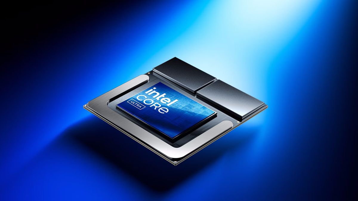
In a surprise move, Intel announced today that it no longer plans to use its own 'Intel 20A' process node with its upcoming Arrow Lake processors for the consumer market. Instead, it will use external nodes, likely from partner TSMC, for all of Arrow Lake's chip components. Intel's only manufacturing responsibilities for the Arrow Lake processors will be packaging the externally manufactured chiplets into the final processor.
The announcement comes as Intel embarks on a vast restructuring in the wake of troubling financial results last quarter. The company continues to lay off 15,000 workers, among the largest workforce reductions in its 56-year history.
The node change comes after Intel initially demoed a wafer of Arrow Lake processors fabbed on the 20A node at its Innovation 2023 event, which indicated the chips were already far along in the development cycle. At the time, Intel said Arrow Lake would come to market in 2024. Since then, industry rumors pointed to the 20A node only being used for a subset of the Arrow Lake family, while the remainder would use a TSMC node.
Intel says its crucial next-gen 'Intel 18A' node remains on track for launch in 2025. It has now shifted its engineering resources from 20A to the newer 18A node, which the company says was spurred by the strength of the yield metrics for 18A. Intel again noted that it had reached a sub-0.40 D0 defect density (def/cm^2) for 18A, a critical measurement of the yield rate for a process node. A process node is usually considered production-worthy and healthy once D0 reaches 0.5 or below.
It appears that Intel will now leapfrog over its 20A process entirely and avoid the capital expenditures required to bring the node to full production. Eliminating the always-eye-watering ramp costs of a new node, particularly one as advanced as 20A, will surely contribute to the company meeting its cost-cutting goals.
The Intel 20A node was never planned for many products due to the company's fast-track move to the more advanced 18A node as it races to meet its goal of delivering five nodes in four years, so building out an extensive 20A production would have limited returns. However, Intel's 20A served as a vehicle for several new advances, like RibbonFet Gate-All-Around (GAA) technology, which is Intel’s first new transistor design since FinFET arrived in 2011. It also marked the debut of the company's PowerVia backside power delivery tech, which routes power for the transistors through the backside of the processor die.
Intel says the learnings it gained from its 20A node have contributed to the success of its 18A node, which makes sense given that 18A is a tighter refinement of the technologies invented for 20A.
Intel notes that it has chips built with the 18A process already powered on in the lab and booting operating systems and also touted that it has now delivered its critical PDK 1.0 to customers. This key design framework will allow external customers to build chips using Intel process nodes, a critical component of Intel's IDM 2.0 turnaround plan, which hinges on the company becoming an external foundry that produces chips for external customers.
Microsoft and the U.S. Department of Defense have already signed on to produce chips using the 18A node, and Intel plans to have eight tape-ins by the middle of 2025.

:quality(85):upscale()/2024/10/17/848/n/1922729/9dece426671163b35dcb11.60305022_.jpg)


 English (US) ·