
 8 months ago
112
8 months ago
112
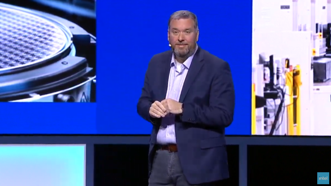
At its Vision 2025 conference, Intel announced today that it has entered risk production of its 18A process node. This crucial production milestone signifies that the node is now in the early stages of low-volume test manufacturing runs. Intel's Kevin O'Buckley, the Senior Vice President of Foundry Services, made the announcement as Intel nears the full completion of its "five nodes in four years" (5N4Y) plan that was originally set in motion by ex-CEO Pat Gelsinger as part of the company's quest to retake the semiconductor crown from rival TSMC. The conference also marks the first time that new CEO Lip-Bu Tan has taken to the stage as the new leader of Intel.
Intel originally announced its four-year plan in June 2021, and despite canceling high volume manufacturing of the 20A node as a cost-cutting measure, Intel is on the cusp of reaching the finish line with its 18A node. Notably, Intel's 5N4Y plan hinged on the process nodes being available for production rather than actively being in the final high volume manufacturing (HVM) stage.
"Risk production, while it sounds scary, is actually an industry standard terminology, and the importance of risk production is we've gotten the technology to a point where we're freezing it," O'Buckley explained. "Our customers have validated that, 'Yep, 18 A is good enough for my product.' And we have to now do the 'risk' part, which is to scale it from making hundreds of units per day to thousands, tens of thousands, and then hundreds of thousands. So risk production [..] is scaling our manufacturing up and ensuring that we can meet not just the capabilities of the technology, but the capabilities at scale."
Risk production is one of many steps on the long road to fielding a new process node and indicates that the company believes the node is nearly ready for HVM. Intel has already produced plenty of 18A test chips/shuttles, typically wherein multiple different designs are prototyped on a single wafer. In contrast, risk production consists of pressing full wafers of chip designs into low-volume manufacturing as the company tweaks its manufacturing flow and qualifies the node and Process Design Kit (PDK) in real-world production runs. Intel will then scale production up to higher levels in the second half of the year. This step of bringing up a semiconductor process comes after the R&D, design, and prototyping stages of development.
There is some 'risk' to risk production, though, as yields and functionality (parametric yields, etc.) can be sub-par as the company refines its manufacturing techniques and optimizes its tooling as it works up the learning curve. As such, customers typically use risk production to manufacture qualification or engineering samples, and the customers aren't given as stringent yield targets/guarantees as they are with nodes fully qualified for HVM. However, some customers are willing to assume those risks to get the payoff of gaining significant time-to-market advantages through early access to the node, which then allows them to adjust and perfect their designs before competitors even begin production.
Intel hasn't yet specified if the 18A risk production is for its own Panther Lake processors, which it says will arrive on schedule later this year, or if the production runs are for its external foundry customers. However, Panther Lake, Intel's first 18A processors, will enter mass production later this year. As such, the Panther Lake chips are likely the risk production subject; this schedule generally aligns with our expectations for a typical risk production-to-HVM timeline for Intel.
Although Intel pioneered several new technologies on its cancelled 20A node, the 18A (1.8nm) chips will be the first productized chips with both PowerVia backside power delivery and RibbonFET gate-all-around (GAA) transistors. PowerVia provides optimized power routing to improve performance and transistor density, and RibbonFET also provides better transistor density along with faster transistor switching, but in a smaller area.
Intel also continues to work on its broader foundry roadmap, which includes the follow-on 14A node, Intel's first to utilize High-NA EUV lithography. Numerous node extensions to other nodes will further expand Intel Foundry Services' portfolio to a broader range of applications.
These developments come during turbulence at Intel Foundry as the company adjusts to changing macroeconomic factors. Intel recently delayed the build-out of its Ohio operations until 2030, for example. However, the announcement of 18A risk production mirrors the positive reports that Intel is running its first 18A wafers through its Arizona fabs.
We expect to learn much more about Intel's future plans at its Foundry Direct Connect event in late April.


 English (US) ·