
 1 month ago
58
1 month ago
58
The artificial intelligence industry is developing so rapidly that the leading suppliers of AI accelerators — AMD and Nvidia — have moved to a yearly product release cadence. Furthermore, it appears that hyperscalers who can afford to develop their own silicon followed suit, so Amazon Web Services, Google, and Meta are also going to release new AI accelerators every year through to the late 2020s.
But which processors are on the horizon? We drew the big picture of the AI and HPC accelerator industry over the next several years. Here's what that looks like.
Swipe to scroll horizontally
| Row 0 - Cell 0 | 2022 | 2023 | 2024 | 2025 | 2026 | 2027 |
AMD | MI250X | MI300X | MI325X | MI350X/355X | MI430X | MI450X | MI500X |
Amazon | Trainium 1 | Trainium 2 / Inferentia 2 | Trainium 2 Ultra | Trainium 3 | Trainium 3 Ultra | Trainium 4 |
TPU v5e | TPU v5p | Trillium | Ironwood (v7?) | TPU v8p | TPU v8e | TPU v9? | |
Intel | Gaudi 2 | - | Gaudi 3 | Gaudi 4 | Falcon Shores | Jaguar Shores |
Microsoft | - | Maia 100 | - | - | Braga (Maia 200) | Clea (Maia 300) |
Nvidia | H100 | H200 | B100/B200 | Rubin (VR200) | Rubin Ultra (VR300) | Feynman |
OpenAI | - | - | - | - | Custom XPU | ? |
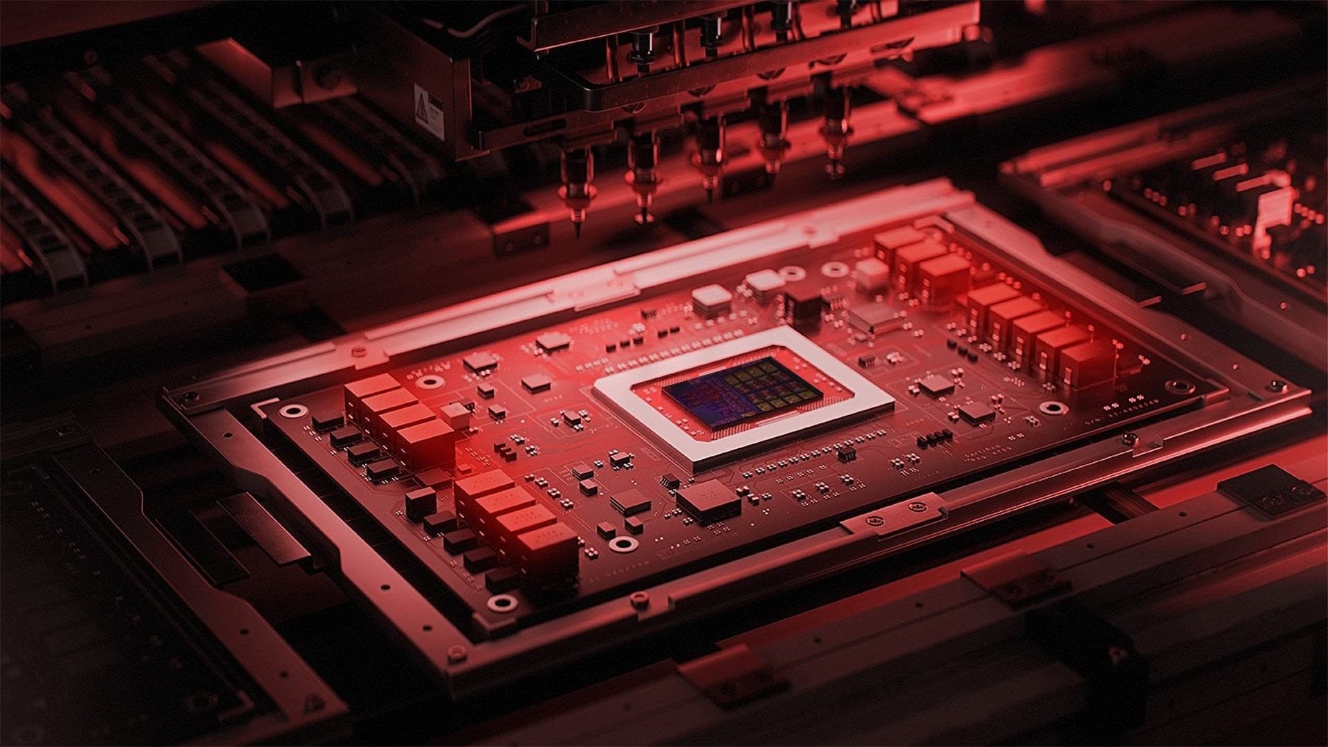
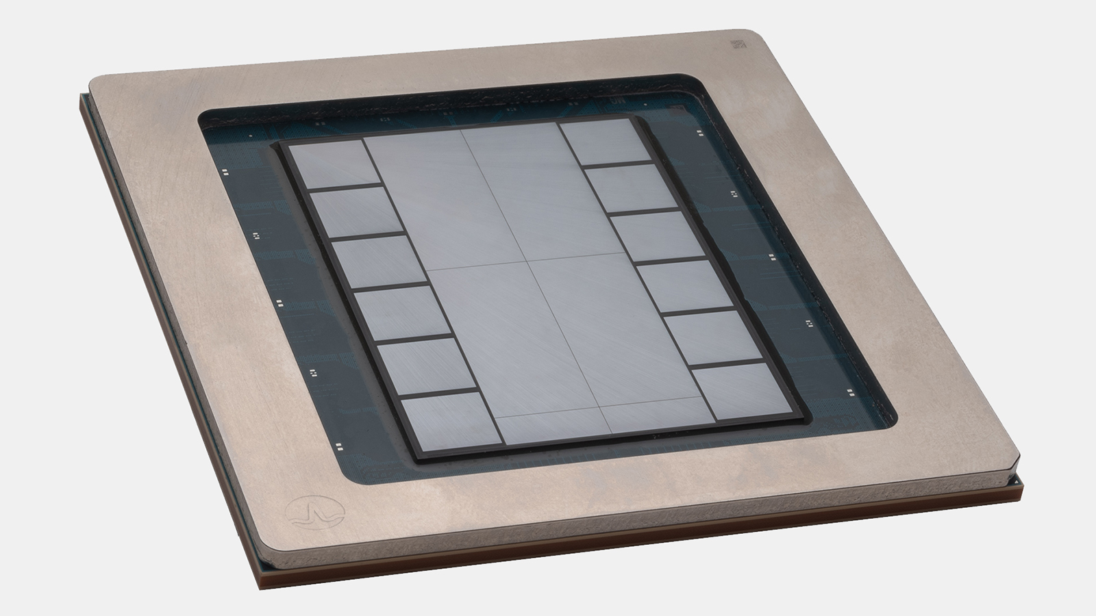
AMD
Traditionally, high-performance AI and HPC accelerators from the early 2020s — such as AMD's Instinct MI100 and MI200-series, and Nvidia's A100 and H100-series — were essentially the same product. This is perhaps why many hyperscalers have decided to build their own custom accelerators, dedicated specifically to AI workloads, to optimize costs, performance, and power consumption.
While Nvidia's Blackwell and Blackwell Ultra GPUs are tailored primarily for AI and FP32 and FP64 performance, they're not competitive in HPC because they lack sufficient FPUs with appropriate capabilities. AMD's latest Instinct MI350-series is still aimed at both AI and HPC workloads. Luckily, the new lineup of AMD's compute GPUs supports FP4 and FP6 data formats for AI inference, but since the GPU also supports FP64, the company had to sacrifice some performance in lower-precision workloads.
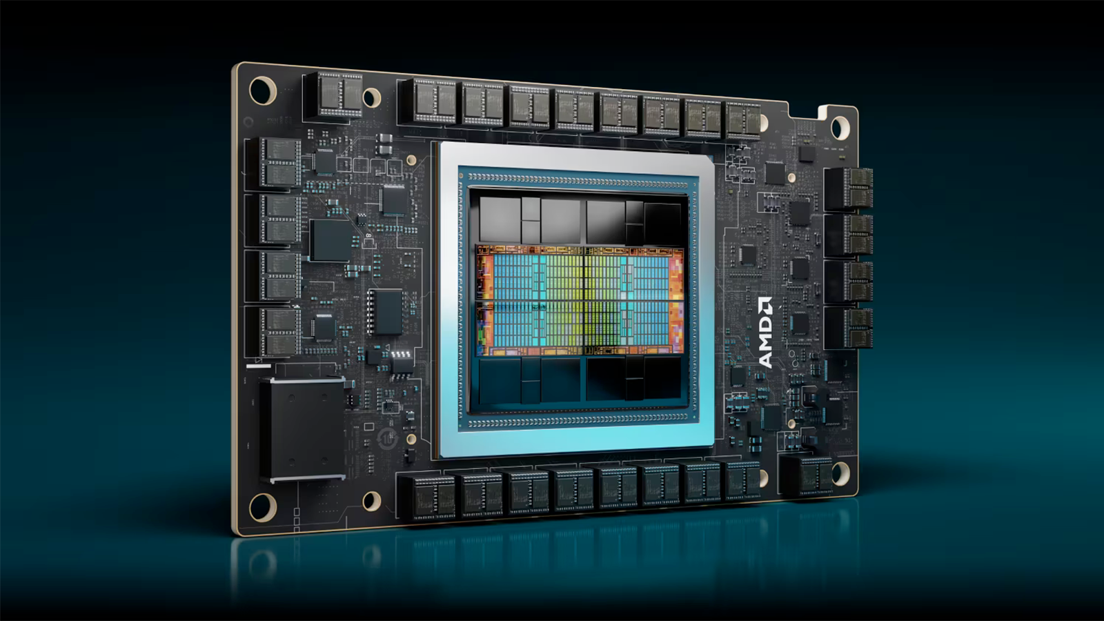
However, things are going to change for AMD with the Instinct MI400-series, set to land sometime in the second half of 2026. The upcoming MI450X will focus on AI workloads, while the MI430X will target traditional supercomputing applications. Both processors are expected to be made using TSMC's N2 (2nm-class) fabrication process, packaged using CoWoS-L technology, and equipped with HBM4 memory.
Each Instinct MI400-series processor will be built on different subsets of AMD’s CDNA Next architecture, according to reports. The MI450X will focus on low-precision formats such as FP4, FP8, and BF16, while the MI430X will support high-precision formats like FP32 and FP64. This separation is expected to help AMD eliminate unnecessary compute blocks from each chip, thus ensuring more efficient use of silicon and better tuning for specific workloads.
Both accelerators will include Infinity Fabric and UALink connectivity. While this makes them among the first GPUs to integrate UALink, adoption is expected to be limited at launch because external partners like Astera Labs, Auradine, Enfabrica, and XConn are not expected to have switching hardware ready by the second half of 2026.
Without these switches, large-scale deployments using UALink will not be possible in 2026, restricting systems to small-scale topologies like mesh and torus. Nonetheless, AMD will still offer its Helios rack-scale solution with 72 GPUs, which will scale out using Ultra Ethernet technology already supported by existing network cards, including AMD's own Pensando Pollara 400 and the upcoming Pensando Vulcano cards.
AMD's Instinct MI400-series will be followed by the Instinct MI500-series GPUs, which are expected to hit the market in 2027. Therefore, expect MI500 processors to be made on TSMC's N2 production node and packaged using CoWoS-L, though it remains to be seen whether AMD adopts HBM4E for these units. The Instinct MI500-series processors will power AMD's next-generation AI rack-scale solution, which will carry 256 GPUs..
Amazon
Amazon exclusively uses its AI accelerators at its own data centers, so the company does not disclose too many details about its two chips. Amazon uses its Trainium chips for both training and inference, its Inferentia chips solely for inference workloads.
Amazon has successfully deployed at least two generations of Trainium and Inferentia processors, including the latest Trainium2 Ultra (667 BF16 TFLOPS, 1300 FP8 TFLOPS, 96 GB of HBM3E, CoWoS-R). Interestingly, it appears that Amazon does not have plans to build more Inferentia processors in the coming years, as it intends to focus on Trainium. However, this change has not been officially confirmed by the company, and it remains a rumor.
Amazon's plans for late 2025 – early 2026 include Trainium3, which is expected to offer higher performance, support for new data formats, and up to 128 GB of HBM3E memory onboard. The chip is expected to be produced by TSMC on one of its 3nm-class nodes, most likely N3P. The Trainium3 chip will be followed by Trainium3 Ultra, featuring 128 GB of HBM4 in 2026 - 2027, which will further increase performance. After that, expect Amazon to release a 2nm-based Trainium4 chip in 2027 – 2028, though there are currently no details on estimated performance or features.
Google has been developing its AI accelerators since 2015, meticulously increasing performance and adding features to its performance (e.g., TPU v5p) and efficient (e.g., TPU v5e) tensor processing units (TPUs).
Last year, the company introduced its Trillium (TPU v6e) chip, equipped with 32GB of HBM3, aimed primarily at low-power inference workloads. This year, the company rolled out its Ironwood accelerator, its 7th Generation TPU, built for large-scale training and inference workloads. Each chip is made on TSMC's 3nm-class process technology, which features 4,614 FP8 TFLOPS performance (10 times more than its predecessor, TPU v5p, but only slightly higher than Nvidia's H100) and comes with 192 GB of HBM3E.
The unit delivers 7.37 TB/s of HBM bandwidth, around 2.64 times that of v5p, and 1.2 TB/s bidirectional Inter-Chip Interconnect (ICI) bandwidth. Ironwood pods scale up to 9,216 chips, delivering a total of 42.5 FP8 ExaFLOPS, which makes it one of the most powerful systems built to date. In terms of efficiency, Ironwood offers around two times better performance per watt compared to Trillium, and is nearly 30 times more power efficient than Google’s first Cloud TPU.
After Ironwood (TPU v7p), Google is expected to release its 8th Generation TPUs — v8p and v8e — which are rumored to be made on TSMC's 3nm-class process technology and feature up to 288 GB of HBM3E memory. So, do not expect a major performance increase from these parts. Google's v8p and v8e accelerators are slated for 2026.
Google's TPUs will likely see a major performance increase in 2027 or 2028, when the company rolls out its 9th Generation TPU based on an all-new architecture with HBM4 memory. These parts are projected to be created using TSMC's N2 fabrication process and use CoWoS-L packaging, which suggests very high internal bandwidth for system-in-packages. Some believe that TSMC and Google might even adopt hybrid bonding, but that remains to be seen.
Intel
Although Intel's CPUs are widely used in AI servers, it does not look like its Gaudi 3 accelerators have gained any traction so far. While multiple loyal partners offer Gaudi 3-based servers, with Dell offering a workstation with a Gaudi 3 card, the company's share of the AI accelerator market is negligible.
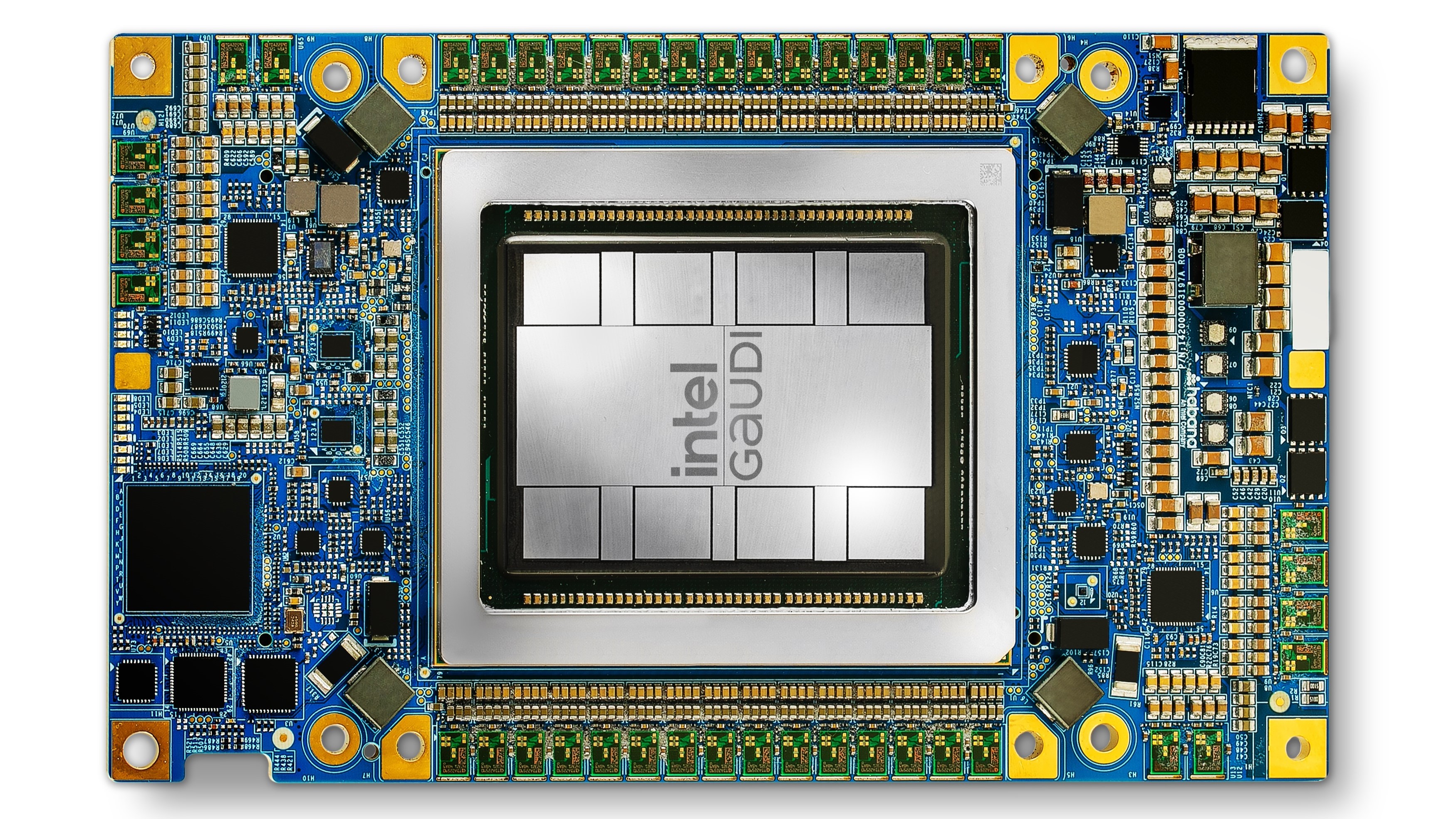
One reason large companies might hesitate to develop or deploy AI models for Gaudi is that Intel has already announced Gaudi will be discontinued when it launches its AI GPUs in 2026 – 2027. Investing tens of millions of dollars in a platform set to go extinct in a couple of years is not something big players do, so Gaudi is unlikely to take off. In fact, it remains to be seen whether it ever releases a refresh for its Gaudi 3 processor.
As for Intel's GPU plans, the firm will use its codenamed Falcon Shores GPU for internal development purposes, and may offer access to select AI companies. Intel's first compute GPU for AI workloads, codenamed Jaguar Shores, will be available to a wide range of clients and is set to be released in 2027.
Although Meta is among the leaders when it comes to hardware investment in AI, the company's in-house AI silicon efforts are behind those of its rivals. Meta's own AI chips are called Meta Training and Inference Accelerators (MTIA). They are developed in collaboration with Andes, which provides RISC-V-based processing elements (PEs), and Broadcom, which designs processors that use a systolic array architecture.
Meta's 1st Generation MTIA v1 was introduced in 2023: it used a chip built by TSMC on its 7nm-class process technology, and was equipped with 64GB of LPDDR5 memory. Meta itself stated that MTIA v1 was deployed in its data centers and was used to serve recommendation and ranking models in production.
However, that deployment seems limited to internal workloads and was not necessarily at the scale one would expect for a full infrastructure shift. The company's more recent MTIA chips are made on TSMC's 5nm-class fabrication process and double onboard memory to 128 GB (MTIA 2) and 256 GB (MTIA 2.5). However, the company will get more aggressive with subsequent generations of MTIA.
Meta's MTIA v3 — due in 2026 — is projected to be a considerably higher-performance solution, as it's expected to use a compute chiplet made on TSMC's N3 fabrication process, and is expected to use HBM3E memory. The company is also expected to release MTIA v4 in 2027. This accelerator will likely use two or more chiplets fabbed on TSMC's 2nm fabrication process and equipped with HBM4 memory.
Microsoft
Microsoft was a bit late to the custom AI silicon party with its its Maia 100-series launching in late 2023, years after Amazon, Google, and Meta. Maia 100 is built on a 5nm-class production node by TSMC, contains 105 billion transistors, and is equipped with 64 GB of HBM2E memory.
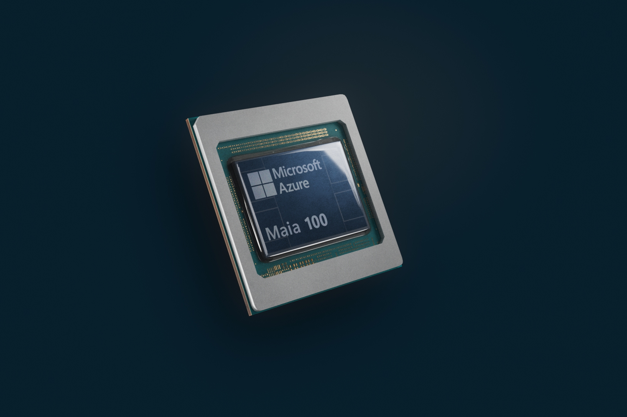
According to Microsoft's own blog, Maia 100 has been deployed in Azure to support large‑scale AI training and inference workloads. However, external reporting suggests that Maia's deployment has not been widespread across Microsoft's entire service infrastructure, and the vast majority of Azure AI services still rely on partner hardware, such as GPUs from AMD and Nvidia.
The company is currently working on its next-generation Maia processors: the codenamed Braga (Maia 200?) chip will use TSMC's 3nm node and HBM4 memory. Braga is allegedly due in 2026, with its successor, Clea (Maia 300?), due at a later date. However, considering the limited adoption of Maia, Microsoft might want to recalibrate the positioning of its own AI accelerators to reduce complexity and risk.
Nvidia
While many companies like Broadcom and Marvell develop XPUs for AI workloads, Nvidia continues to lead the market for both training and inference workloads. The company's latest Blackwell Ultra architecture sacrifices INT8, FP32, and FP64 performance in favor of NVFP4 performance, mainly used for inference. So, Nvidia is certainly doing everything to keep its crown as the dominant force in the AI industry.
Nvidia's upcoming data center GPU carries the codename Rubin, and is expected in late 2026. The initial model, tentatively referred to as R100/R200, will consist of two reticle-sized GPU dies and two dedicated I/O chiplets, all built using TSMC's 3nm-class node, likely N3P or something customized for Nvidia's needs. Memory-wise, it will integrate 288 GB of HBM4 across eight stacks, each running at 6.4 GT/s, yielding an impressive ~13 TB/s of total memory bandwidth.
The R100/R200 is designed primarily for AI acceleration; it is expected to hit 50 PFLOPS of NVFP4 performance for inference, and roughly 17 FP8 TFLOPS for training workloads. Performance data for other formats has yet to be shared, but incremental improvements across the board are anticipated, relative to the Blackwell generation. This performance uplift will come at a cost: each VR200 unit is projected to draw 1,800 watts, posing new power and cooling demands on data center infrastructure.
But Nvidia's Rubin GPUs for AI will not come alone. Nvidia is also set to offer its Rubin CPX, a newly introduced GPU, which is designed to handle the context phase of long-context inference. This workload is becoming increasingly common in next-generation AI models, which must process up to 1 million tokens before generating output.
Rather than relying solely on high-power, high-bandwidth GPUs like the Rubin R100/R200 (which uses HBM4), CPX offloads this specific task onto a compute-dense (but bandwidth-light) CPX GPU that features 128 GB of GDDR7, offering a cheaper, cooler, and simpler memory alternative to HBM. With 30 petaFLOPS of NVFP4 compute performance, hardware acceleration for attention mechanisms, and even support for video encoding/decoding, CPX is designed specifically for rapid input processing at a relatively low cost and power consumption. Nvidia's Rubin CPX GPU will work alongside Rubin and Vera CPUs in the NVL144 CPX system, which will deliver 8 exaFLOPS of NVFP4 compute and 100 TB of memory per rack.
In 2027, Nvidia plans to introduce a substantially upgraded variant: Rubin Ultra (VR300). This will double the compute complex to four reticle-sized GPU tiles, alongside two I/O dies, and support 1 TB of HBM4E memory made up of 16 stacks, offering a blistering 32 TB/s bandwidth. Targeted FP4 performance is 100 PFLOPS, making it twice as fast as VR200 for inference.
However, the VR300’s scale demands enormous power — 3,600 watts per package — which makes it suitable only for highly specialized, high-density deployments with advanced liquid cooling systems. Nvidia will continue using CoWoS-L packaging for both VR200 and VR300, but the Rubin Ultra variant's footprint requires either TSMC's forthcoming 9.5-reticle CoWoS-L interposer (sized 120 × 150 mm) or an arrangement of stitched smaller interposers, since no vertical die stacking is visible in official slides.
Looking beyond Rubin, Nvidia's 2028 plans include a follow-up GPU family codenamed Feynman. While specific architectural details are unavailable, it is noteworthy that these processors will likely be made on TSMC's A16 process technology with a backside power delivery (which will provide an ultimate uplift both for transistor density and for performance) and are said to adopt next-generation HBM. Whether this refers to a specialized form of HBM4E or early HBM5 is still unclear — though the latter seems premature for that timeframe.
OpenAI
OpenAI is perhaps the most known AI company due to popularity of its ChatGPT service, but for AI hardware, it is a new kid on the block. The company has reportedly been working on its own AI accelerator since at least late 2023 presumably with Broadcom.
Recently, Broadcom confirmed that an undisclosed client intends to procure $10 billion worth of custom AI processors, which are set to be delivered in the third quarter of 2026. While the industry believes that the product in question is OpenAI's first custom AI processor, this has never been formally confirmed.
Although OpenAI will allegedly spend $10 billion procuring custom processors made according to its needs, which may point to 1 – 2 million of XPUs, depending on unit prices, its recent agreement with Nvidia indicates that it will gain access to $100 billion worth of Nvidia GPU hardware, presumably over several generations of GPUs. This suggests that the lion's share of OpenAI's workloads will still rely on Nvidia and its models will be optimized for the CUDA platform.


 English (US) ·