
 1 hour ago
3
1 hour ago
3
Although the performance of high-bandwidth memory (HBM) has increased by an order of magnitude since its inception around a decade ago, many elements have remained fundamentally unchanged between HBM1 and HBM3E. But as the demands for bandwidth-hungry applications evolve, the technology must also change to accommodate them.
In new information revealed at TSMC's European OIP forum in late November, HBM4 and HBM4E will offer four major changes. HBM4 will receive a 2,048-bit interface and base dies produced using advanced logic technologies. Meanwhile, HBM4E will be able to utilize customizable base dies, which can be controlled with custom interfaces. These are dramatic shifts, which will have a big impact sooner than you might think.
HBM4: The next big thing
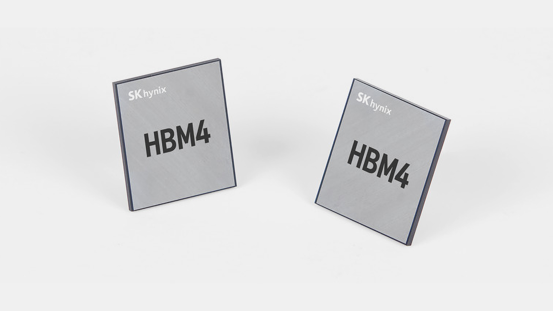
HBM4 — whose specification was officially published earlier this year — is the standard that sets the stage for a number of upcoming innovations in the AI and HPC memory market.
Each HBM4 memory stack features a 2,048-bit interface that officially supports data transfer rates of up to 8 GT/s, though controllers from controller specialists like Rambus and HBM4 stacks from leading DRAM vendors already support speeds of 10 GT/s or higher, since implementers want to have some reserve for additional peace of mind.
A stack with a 2,048-bit interface operating at 12 GT/s can deliver bandwidth of 2 TB/s, so an AI accelerator with eight HBM4 stacks will have access to potential bandwidth of 16 TB/s. And 12 GT/s could be just the beginning. Note that Cadence is already offering an HBM4E physical interface (PHY) with 12.8 GT/s support.
Internally, HBM4 doubles concurrency to 32 independent channels per stack (each split into two pseudo-channels), which reduces bank conflicts and raises efficiency throughput under highly parallel access patterns.
HBM4 stacks also support 24 Gb and 32 Gb DRAM devices and offer configurations for 4-Hi, 8-Hi, 12-Hi, and 16-Hi stacks, thus enabling capacities of up to 64 GB, which allows to build accelerators for next-generation AI models with trillions of parameters. Micron expects 64 GB stacks to become common with HBM4E sometime after late 2027, which aligns with Nvidia plans to equip its Rubin Ultra GPU with 1 TB of HBM4E memory.
The electrical specification of HBM4 broadens operating voltages with vendor-specific VDDQ options between 0.679V and 0.963V and VDDC of 0.97 V or 1.07 V, which enables DRAM makers to bin their offerings for efficiency or frequency while maintaining compatibility with the specification. On the security side of things, HBM4 supports directed refresh management (DRFM) to mitigate row-hammer attacks.

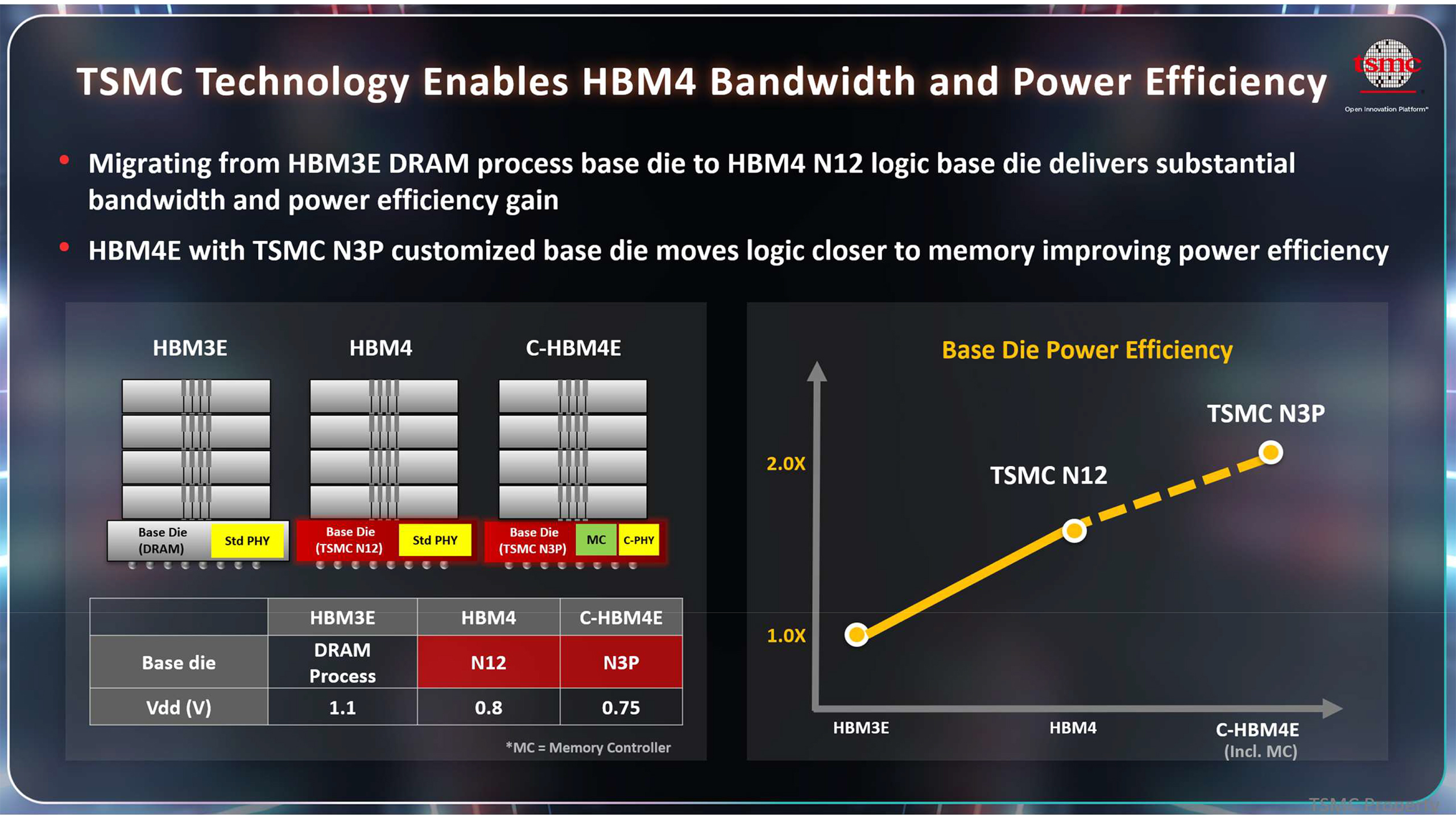
Because HBM4 expands its interface to 2,048 bits, it is supposed to have double the I/O contacts compared to previous-generation HBM stacks. Since it was close to impossible to produce a base die with proper routing using DRAM process technologies, memory makers like Micron, Samsung, and SK hynix collaborated with TSMC early on to ensure compatibility with CoWoS packaging technologies and to produce HBM4 base dies using 12FFC or N5 fabrication technologies.
Back then, it was thought that 12FFC would be used for 'regular' HBM4 base dies, which would be integrated with their host processors using advanced 2.5D process technologies, whereas N5 base dies would be used for HBM4 memory, which would then be integrated using direct bonding on logic chips.
At the European OIP 2025 forum, neither TSMC nor its partners mentioned N5-based HBM4 base dies for integration using hybrid bonding or similar technologies, which likely means that the project is not exactly a priority for now.
Potentially, the integration of HBM4 memory stacks on top of a high-performance processor creates significant thermal density, which would make it difficult to cool. It's also possible that hot compute chips can damage hot DRAM devices, and vice versa, but this is merely speculation.
There may also be hybrid-bonded SoIC-X 3D integrations, with stacked HBM4 on top of compute chiplets in development, but their developers do not want to share results just yet.
In any case, HBM4 base dies made by TSMC on its low-power 12FFC or N5 process technologies, as well as custom C-HBM4E base dies produced on TSMC's N3P node use lower voltages (0.8V – 0.75V vs 1.1V in case of HBM3E), and are up to two times more power efficient than base dies of HBM3E memory manufactured using DRAM technologies, according to TSMC.
On the other hand, since HBM4 requires a more sophisticated controller and a larger, more complex PHY compared to HBM3E (15mm^2 vs 11mm^2, according to GUC). HBM4's memory subsystems will be more power hungry than HBM3E subsystems, too. However, due to considerably higher bandwidth, enabled by HBM4, they will be considerably more power and area-efficient than predecessors.
As for IP readiness, GUC has taped out its HBM4 PHY IP on N3P in March 2025. This will be validated with HBM4 memory samples in Q1 2026, when the company will be formally able to claim that it has a silicon-proven and validated HBM4 memory solution. Additionally, the IP will be compatible with all types of CoWoS packaging (-S, -R, -L) and can address a variety of applications. HBM4 memory controllers are available from a range of companies, including Rambus. EDA developers like Cadence, Siemens EDA, and Synopsys.
HBM4E: 2.5X higher bandwidth than HBM3E
With the introduction of HBM4's 2,048-bit memory interface, JEDEC members had to slash maximum data transfer rates to 8 GT/s from around 9.4 GT/s supported by HBM3E, which still enables a dramatic bandwidth increase. However, HBM4E is set to push electrical and signaling limits higher by supporting per-pin data rates to 12 GT/s (by refining PHY for better signal margin and jitter control at higher frequencies) and extending total stack bandwidth to around 3 TB/s, while keeping the 2,048-bit interface and 32-channel architecture. As a result, the bandwidth offered by HBM4E stacks will be 2.5X higher compared to HBM3E, and even when area and PHY power are taken into account, HBM4E will be 1.7X more power efficient and 1.8X area efficient, according to GUC.
Swipe to scroll horizontally
| Row 0 - Cell 0 | HBM3E | HBM4E | Difference |
Process availability | 7nm, 5/4nm, 3nm | 3nm, 2nm | Row 1 - Cell 3 |
I/O width, Channels | 1024-bit, 16 channels | 2048-bit, 32 channels | 2x |
Speed per pin | 9.4 Gbps | 12 Gbps | 1.3x |
Total bandwidth | 1.2 TB/s | 3 TB/s | 2.5x |
PHY size | 11 mm² | 15 mm² | 1.4x |
PHY power | 6 W | 9 W | 1.5x |
Standard HBM4E solutions will likely be able to use HBM4 base dies, though some memory makers may migrate to base dies using the N5 or N3P process technologies for higher performance and efficiency.
C-HBM4E: The first custom type of memory for AI and HPC
Virtually all leading DRAM makers have introduced proprietary DRAM solutions with certain levels of customization over the past decade, but none of them have gained traction. Starting with HBM4E, HBM memory will get a separate branch of customized solutions, which is set to feature unique capabilities and proprietary interfaces.
On a high level, C-HBM4E is an HBM4E memory stack with a custom base die. The stack retains standard HBM4E memory devices, which comply with clock and electrical requirements set by JEDEC. However, the base die can now be customized in several different ways, thus shifting emphasis from raw bandwidth to the integration of custom logic directly into memory devices, which can be achieved using several methods.
The easiest way — described by Rambus — is to retain the standard HBM4E interface, alongside built-in custom logic and/or caches on the base die, to add features or performance. As long as the HBM4E protocol with supporting firmware and software stacks is compliant, this may increase the performance of memory subsystems beyond increasing transfer rates or widening I/O.
A more complex method— envisioned by TSMC and Rambus — is to place the HBM4E memory controller and a custom die-to-die interface directly into the logic base die. A large part of the industry's focus is on reducing the number of traces required between the processor and the HBM base die, and a custom D2D interface will do just that. By shrinking the interface width, each memory stack consumes fewer I/O pins, which enables a single SoC to attach a greater number of HBM stacks without increasing package size or complexity.
A custom die made using TSMC's N3P technology would allow packing in an HBM4E memory controller, a custom D2D PHY, and potentially some additional logic. For example, KAIST envisions integration of near memory compute (NMC) processors, which will make at least some C-HBM4E solutions system-on-chips (SoCs) with basic processing capabilities.
If near-memory compute logic is indeed integrated into C-HBM4E, the software stack must evolve to become topology-aware and memory-aware, rather than treating a C-HBM4E stack as 'just' memory. Without changes to toolchains, drivers, and runtimes, near-memory compute becomes invisible silicon—present in hardware, but unused by software.
Runtime systems and compilers will need explicit knowledge of bank structure, channel placement, and in-memory execution units so that workloads can be scheduled where data physically resides, instead of being moved across the fabric. In addition to this, programming models will also need extensions to work with in-memory compute, or multi-tier memory systems in general. Finally, operating systems must support heterogeneous memory domains with non-uniform latency and asymmetric coherence, while profilers must observe and optimize execution occurring inside memory devices.
A vision beyond
If the figures published by TSMC and GUC are to be believed, then HBM's raw performance is set to increase by around 2.5 times within the next few years, thanks to HBM4E. This development opens the doors to memory subsystems with a 1 TB capacity and a whopping bandwidth of 48 TB/s. If custom compute logic inside base dies of HBM gets adopted by the industry, this might be the biggest shift in how computers work in decades.


 English (US) ·