
 3 weeks ago
43
3 weeks ago
43
Elon Musk is thinking about outsourcing some of Tesla’s chip production to Intel Foundry and even establishing the company’s own chip production operation, he said at the company’s Annual Shareholder Meeting event. Musk is perhaps the first executive of a big company to consider building an entire semiconductor production facility due to the extreme complexities and costs associated with such a project. Jensen Huang, chief executive of Nvidia, already reacted to Musk’s musings, noting that the head of Tesla may be underestimating the challenge.
“I think we may have to do a Tesla TeraFab,” Musk said. “It is like [TSMC’s] Giga[fab] but way bigger.”
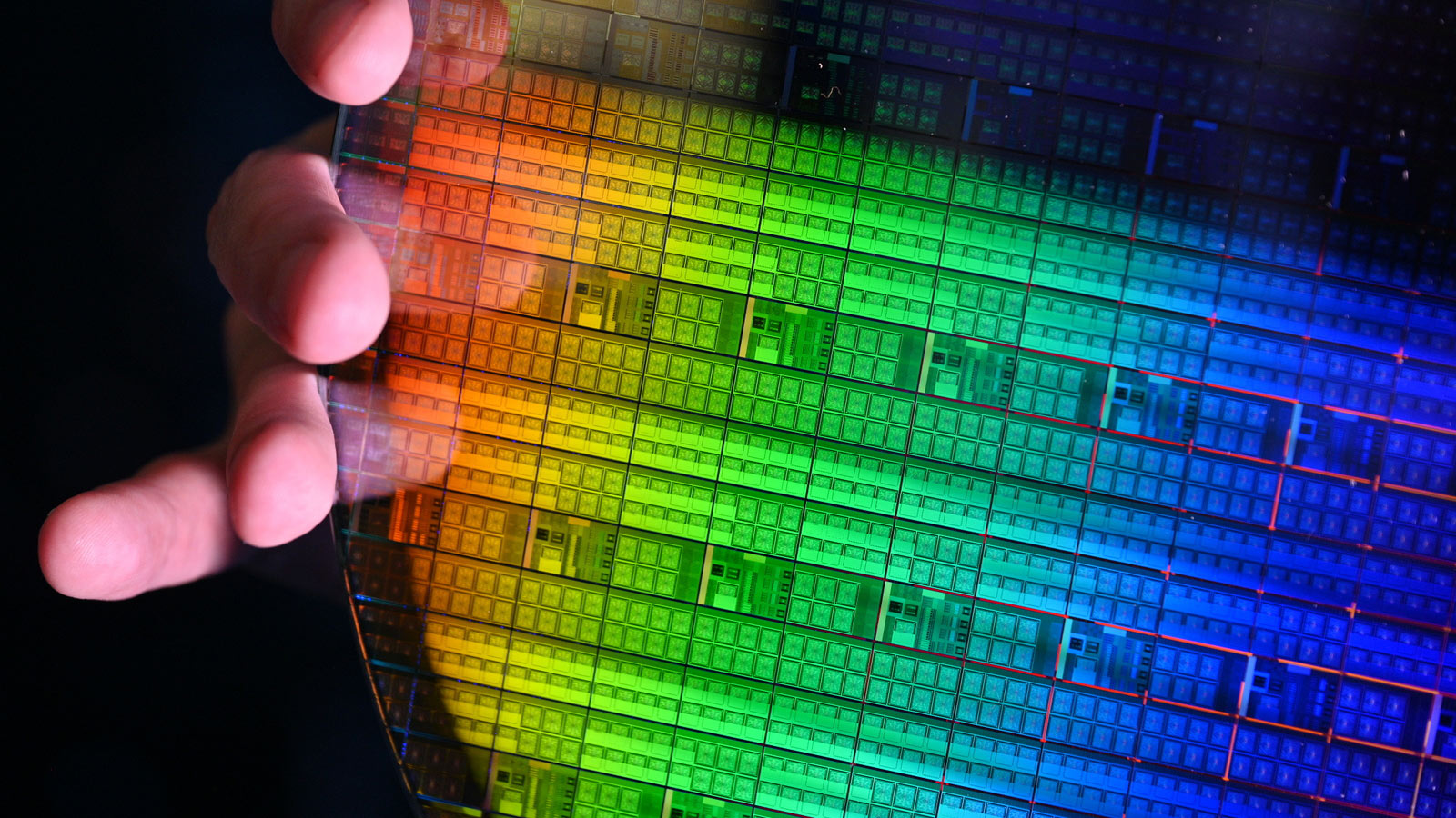
TSMC calls its fab complexes with production capacity from 30,000 to 100,000 wafer starts per month ‘Megafabs’, whereas fab complexes with production capacities of over 100,000 WSPM are referred to as ‘Gigafabs.’ A ‘Terafab’ would mean capacity way beyond 100,000 WSPM, which would transform Tesla into one of the industry’s biggest chipmakers. To put the capacity into context: TSMC’s Fab 21 complex in Arizona — which will cost the foundry $165 billion in total — is expected to become a Gigafab with six fabs, two advanced packaging facilities, and an R&D center. Apparently, Musk is eyeing something bigger. But let us decode the whole story first, as it takes more than money to become a chipmaker these days.
“Building advanced chip manufacturing is extremely hard,” Jensen Huang, chief executive of Nvidia, said at a TSMC event on Thursday. “It is not just build the plant, but the engineering, the science, and the artistry of doing what TSMC does for a living is extremely hard.”
3/5 Jensen on Elon Musk’s chip fab plan: “Building advanced chip manufacturing is extremely hard. It’s not just build the plant, but the engineering, the science and the artistry of doing what TSMC does for a living is extremely hard. $NVDA $TSLA $TSMNovember 7, 2025
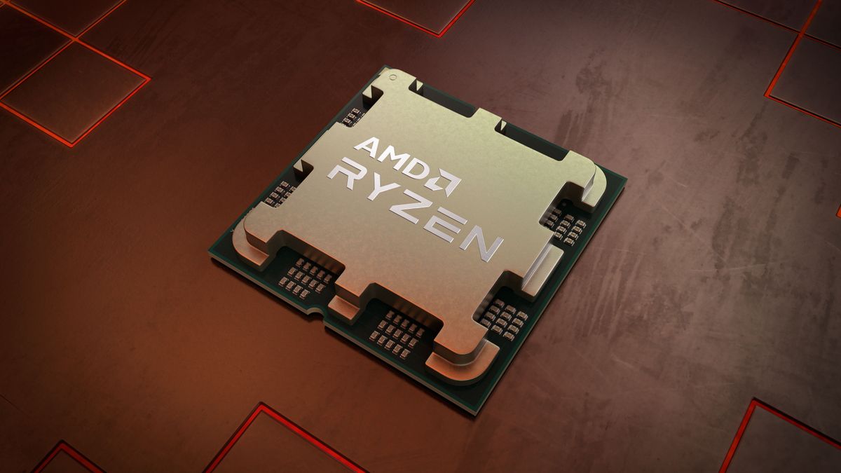
Tesla needs chips
As a major carmaker that also owns some of the industry's largest AI supercomputers, Tesla needs a steady supply of high-performance processors to power its artificial intelligence efforts. The company already uses tens of thousands of Nvidia GPUs, and now that its Dojo project has been cancelled, it plans to use its AI5 processors for cars and robots in its data centers as well. To get plenty of these processors, Tesla plans to double-source them from TSMC and Samsung. Musk also mentioned tapping Intel for chip production, though this might be a bit challenging as the company does not have any automotive-grade process technologies.
“One of the things I am trying to figure out is how do we make enough chips,” Musk asked rhetorically during his keynote speech at the Tesla event. “So, I have a lot of respect for the Tesla partners, TSMC and Samsung, you know, maybe we will do something with Intel. We have not signed any deal, but it is probably worth having discussions with Intel.”
However, he believes that his company will need more AI processors in the long term, which will necessitate building its own chipmaking operations, essentially becoming an integrated device manufacturer (IDM), a role that even established chip designers like AMD, Fujitsu, IBM, and Panasonic gave up in recent decades.
“Even when we extrapolate the best-case scenario for chip production from our suppliers, it is still not enough,” Musk told the audience. “So, I think we may have to do a Tesla TeraFab. It is like [TSMC’s] Giga[fab] but way bigger. I cannot see any other way to get to the volume of chips that we are looking for, so I think we are probably going to have to build a gigantic chip fab. It’s gotta be done.”
Becoming a chipmaker
It costs leading-edge chipmakers billions of dollars to develop a fabrication process and tens of billions to build a single fab with a 20,000 WSPM capacity capable of making chips on a state-of-the-art process technology.
Rapidus — Japan’s first new chipmaker with plans to build chips on advanced nodes in decades — estimates that it needs around ¥5 trillion (about $32 billion) in total investment to develop a process technology and build a fab capable of commercial production of 2 nm-class chips in 2027. While we can only applaud this ambitious project, it remains to be seen whether becoming a leading chipmaker from scratch is possible in the 2020s and with leading-edge nodes.
Developing a new process technology from scratch is a particularly complex, multidisciplinary endeavor that takes 5 or more years these days, from inception to yield ramp. A development cycle of a fabrication technology begins with pathfinding, materials research, transistor structure development, and then running countless TCAD simulations to model doping, strain, and leakage for a new transistor.
Rapidus has licensed its 2nm GAA transistor structure from IBM, but it is also possible to license a chunk of similar technologies from imec and CEA-Leti, public-private R&D institutes. But while it is hard to overestimate the importance of the right transistor structure, this is only the start.
Once transistor technology is complete, engineers build thousands of tightly coupled process steps organized into FEOL, MOL, and BEOL modules — covering transistor formation, interconnects, and metallization. Each of these steps demands atomic-level precision in deposition, etch, lithography, and anneal. Tuning those steps (each with hundreds, if not thousands, of parameters) for manufacturability, uniformity, reliability, defectivity, power, and performance requires decades of engineering experience and time from the team. At this point, technology providers like IBM, Imec, or CEA-Leti cannot really help.
Once each deposition, etch, implant, lithography, and anneal step is stable in isolation, engineers start combining modules (e.g., transistor gate stack and source/drain) on test wafers and tune their sequencing and temperature budgets to prevent cross-contamination or material degradation. This is essentially when the ordered stack of hundreds of steps that define the node — the process flow — takes shape. Again, these integration recipes are not available for licensing from R&D companies or institutes.
After device performance, power, and yield meet targets, the process must be made design-usable by generating PDKs, SPICE models, verified standard-cell libraries for EDA tools, and IPs for chip designers. At the same time, engineers begin implementing the fabrication process in actual fabs and production lines. That implementation and setting the right parameters for equipment is another challenge that demands experience, not something money can buy.
Finally, fabs must achieve high yields in mass production, which is a hard, long, and iterative process involving plenty of experienced engineers.
Can this all be done from scratch in a mere five years by a newcomer? Rapidus will show in 2027.

Follow Tom's Hardware on Google News, or add us as a preferred source, to get our latest news, analysis, & reviews in your feeds.


 English (US) ·