
 8 months ago
150
8 months ago
150
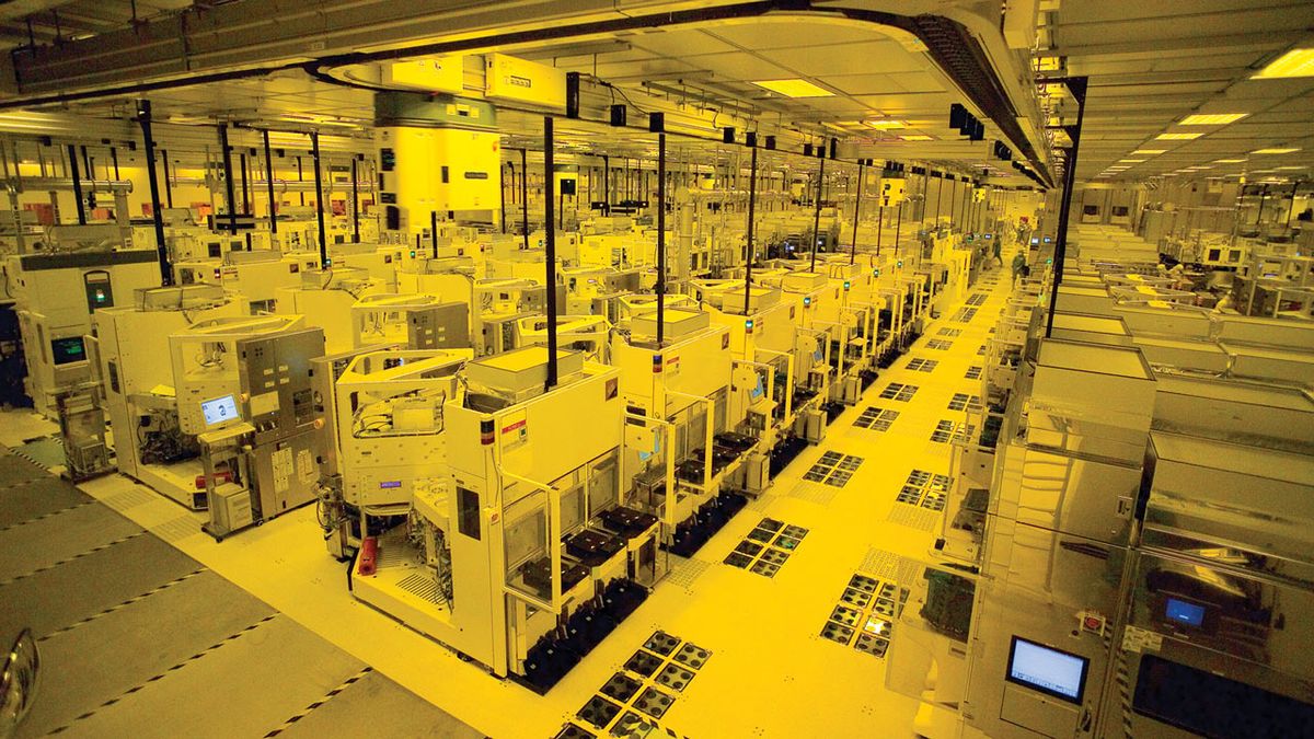
Chinese chipmakers have been gradually shifting some of their production to tools made in China in a bid to support the local wafer fab equipment ecosystem and reduce reliance on tools produced abroad. China already has several well-known manufacturers of chipmaking tools that specialize in one or two types of equipment, which set sales records in 2024. However, there is a little-known Huawei-linked company, Si Carrier Technologies, that has revealed it has almost all types of wafer processing tools in its catalog published at Semicon China and re-published by Zhininren.
SiCarrier Technologies is a startup widely discussed at this year’s Semicon China, but is little known outside of the People’s Republic. The company is closely linked to Huawei and was founded four years ago in Shenzhen to develop world-class fab tools that would compete against front-end chip production equipment made by market leaders ASML, Applied Materials, KLA, and Lam Research, according to Nikkei. SiCarrier's main investor is Shenzhen Major Investment Group, a government-backed fund supporting other chip ventures connected to Huawei, including PengXinWei Integrated Circuit Manufacturing and SwaySure Technology.
SiCarrier currently operates R&D centers in Shanghai, Beijing, Xi’an, Wuhan, Chengdu, Hangzhou, and overseas. Its end-to-end development chain covers materials, components, and full systems. To support rapid development, the company aggressively recruits senior engineers from top global companies like ASML and Applied Materials.
The SiCarrier catalog presented at Semicon China includes a wide range of semiconductor manufacturing equipment, metrology tools, and inspection systems. The catalog does not include any lithography tools (possibly to keep its lithography advancements a secret), but Nikkei reports that the company already has litho tools capable of processing 300-mm wafers on 28nm process technologies and older. Even without lithography machines, the company lists dozens of tools that can perform the vast majority of steps in the front-end semiconductor production flow. The company also has metrology, inspection, and testing tools.
On the process side, the catalog includes tools used for atomic layer deposition (ALD) for dielectrics and metal gates, chemical vapor deposition (CVD), physical vapor deposition (PVD) blanket film deposition and metal contact deposition, epitaxy, etching, and annealing. The catalog does not explicitly characterize tools and their capabilities in terms of actual fabrication processes, but it does frequently refer to ‘advanced process nodes’ as well as ‘future advanced nodes.’
On the metrology and inspection front, the catalog includes tools for the optical inspection of both patterned and unpatterned wafers, atomic force microscopy for morphology inspection at nanoscale resolution, and advanced measurement systems for thin film thickness, element composition, and crystallinity.
Finally, SiCarrier also has various testing machines, including wafer electrical performance tests, known-good die tests, and functional tests. However, these tools are currently aimed mostly at power semiconductors.
For now, it is unclear whether all of the tools that SiCarrier lists can be ordered and acquired. It is also unclear whether these machines are compatible with existing production flows that rely on machines from ASML, Applied, KLA, Lam, TEL, and others.
However, Nikkei claims that SiCarrier has partnered closely with Huawei, which has assembled a large internal team focused on semiconductor manufacturing and equipment, and that they are working to improve process implementation and identify technical challenges across production lines. This could mean that SiCarrier and Huawei intend to build tools for a ‘proprietary’ production flow involving exclusively Chinese tools. If this is the case, it could take years before the first fab with such a flow comes online. Nonetheless, given SiCarrier’s pace so far, it could well impress the industry.


 English (US) ·