
 7 months ago
328
7 months ago
328
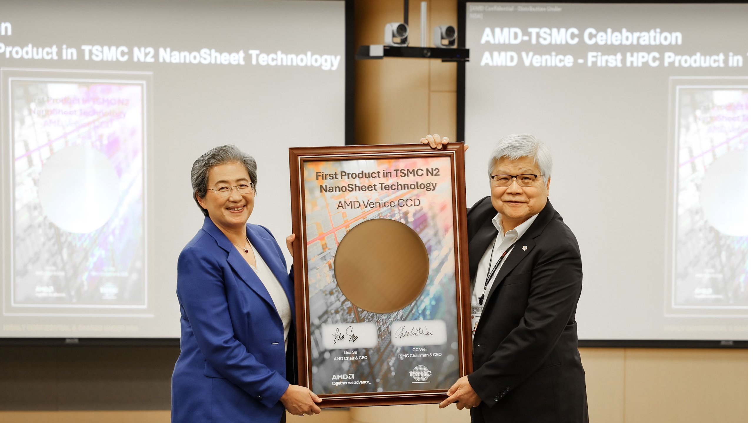
In a rather unexpected turn of events, AMD announced late on Monday that it had obtained its first 2nm-class silicon, a core complex die (CCD) for its 6th Generation EPYC 'Venice' processor, which is expected to launch next year. The Venice CCD is the industry's first HPC CPU design to be taped out on TSMC's N2 process technology, highlighting AMD's aggressive roadmap and the readiness of TSMC's production node.
AMD's 6th Generation EPYC 'Venice' is expected to be based on the company's Zen 6 microarchitecture and is expected to be launched sometime in 2026. The CPU will rely on CCDs to be made on TSMC's N2 (2nm-class) fabrication process, so it is about time for the company to get the first Venice CCDs out of the fab. Yet, the fact that AMD already has chips it can talk about highlights the long-standing collaboration between AMD and TSMC as well as the culmination of joint efforts to build chips on one the most advanced process technologies that TSMC has ever developed to date.
For now, AMD isn't discussing the details of its EPYC 'Venice' processors or CCDs, though the company's press release claims that the silicon had been taped out and brought up, which means that the CCD has successfully powered on and has passed basic functional testing and validation.
"TSMC has been a key partner for many years, and our deep collaboration with their R&D and manufacturing teams has enabled AMD to consistently deliver leadership products that push the limits of high-performance computing," said Dr. Lisa Su, chief executive of AMD. "Being a lead HPC customer for TSMC's N2 process and for TSMC Arizona Fab 21 are great examples of how we are working closely together to drive innovation and deliver the advanced technologies that will power the future of computing."
TSMC's N2 is the foundry's first process technology that relies on gate-all-around (GAA) nanosheet transistors. The company expects its manufacturing technology to offer either a 24% to 35% reduction in power consumption or a 15% increase in performance at constant voltage, along with a 1.15X boost in transistor density compared to the previous N3 (3nm-class) generation. These gains are primarily driven by the new type of transistors and the N2 NanoFlex design-technology co-optimization framework.
AMD's announcement comes after its arch-rival Intel delayed the release of its next-generation Xeon 'Clearwater Forest' processor made on its 18A manufacturing technology (which is set to rival TSMC's N2) to the first half of next year.
Separately, AMD announced that it has successfully validated the silicon of its 5th Generation EPYC processor produced by TSMC at its Fab 21 facility near Phoenix, Arizona. As a result, some of the company's current-generation EPYC CPUs can now be produced in the U.S.
"We are proud to have AMD be a lead HPC customer for our advanced 2nm (N2) process technology and TSMC Arizona fab," said Dr. C.C. Wei, chief executive and chairman of TSMC. "By working together, we are driving significant technology scaling resulting in better performance, power efficiency and yields for high-performance silicon. We look forward to continuing to work closely with AMD to enable the next era of computing."


 English (US) ·