
 3 weeks ago
33
3 weeks ago
33
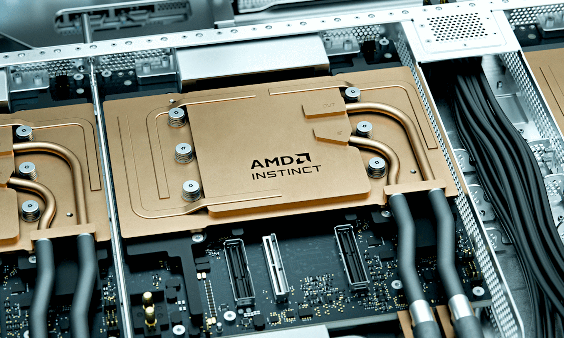
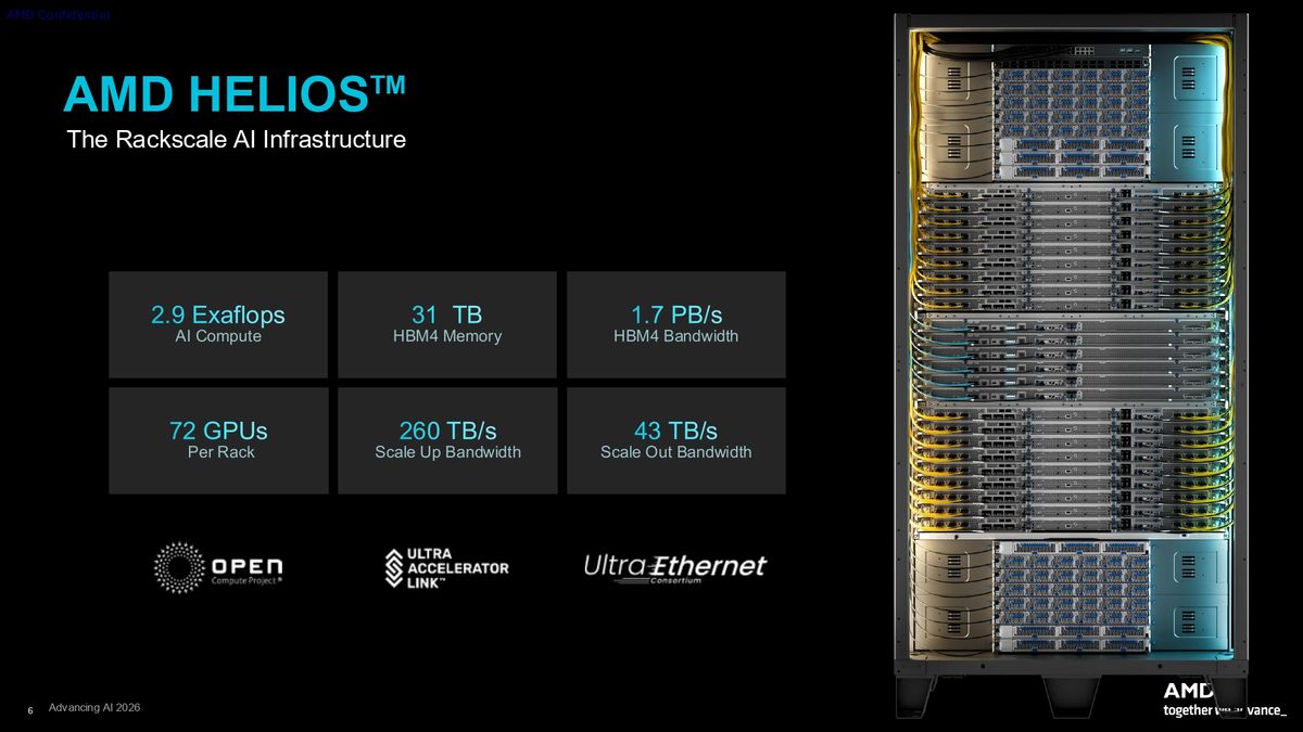
At AMD’s Advancing AI event this week, the company revealed more details of its upcoming MI455X GPU and the Helios rack-scale architecture that will join 72 of those GPUs into a coherent accelerator—the largest such system that AMD has built so far and its first to truly compete with Nvidia’s NVL72 rack-scale design, as used in the Blackwell and Rubin generations.
AMD calls the MI455X “by leaps and bounds the most advanced AI accelerator we’ve ever built,” and from what we’ve seen, it’s the most competitive product at both the chip level and at rack scale that AMD has ever put up against Nvidia’s thorough dominance of the AI compute race.
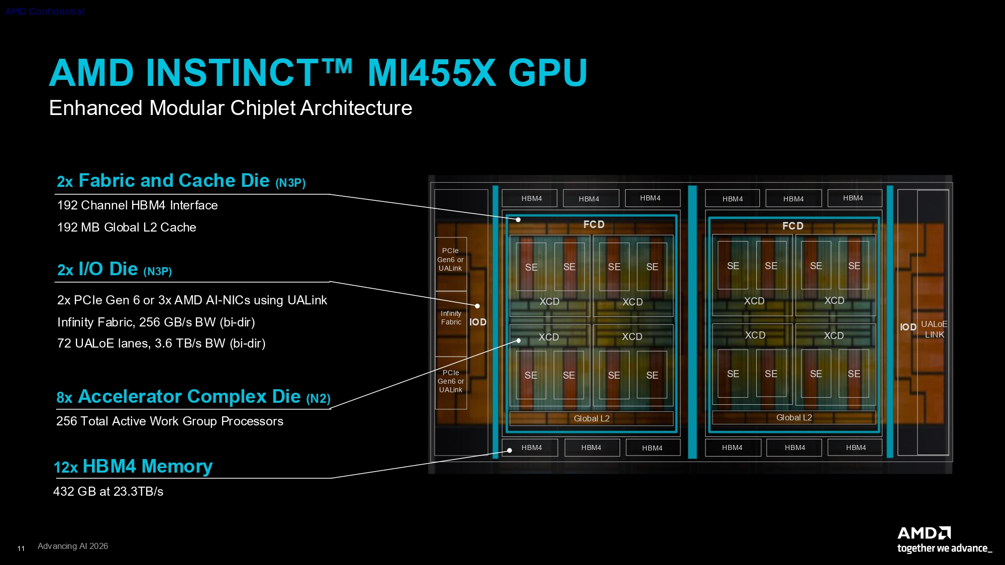
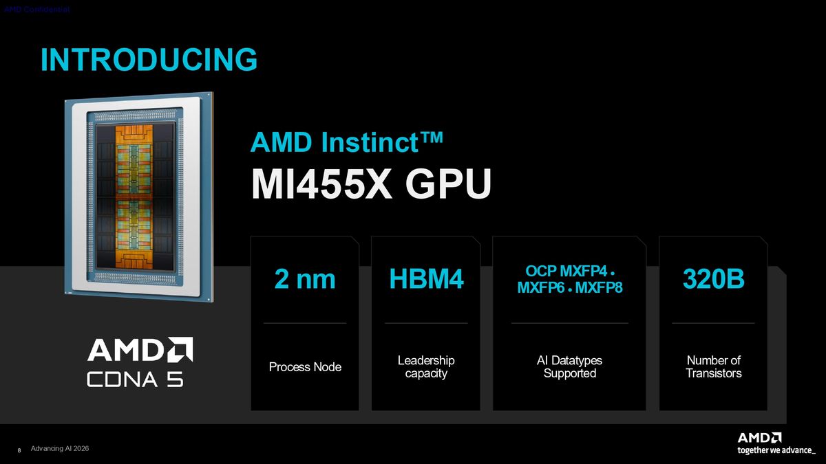
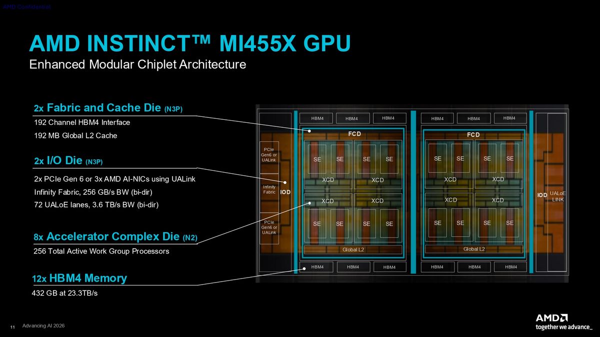
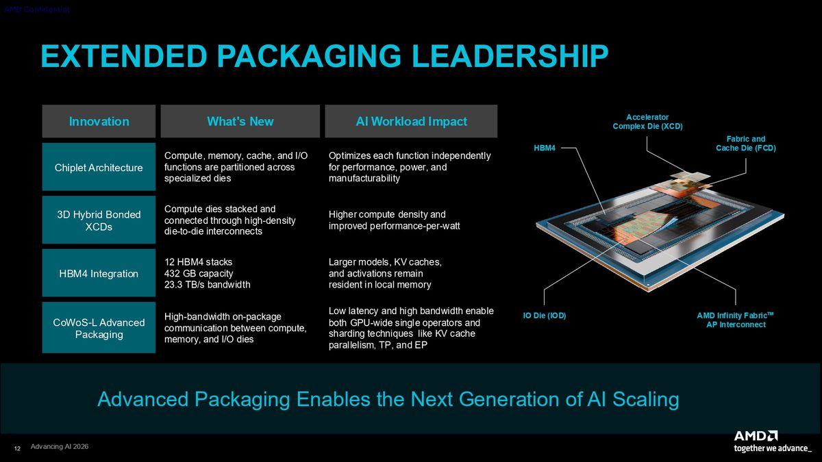
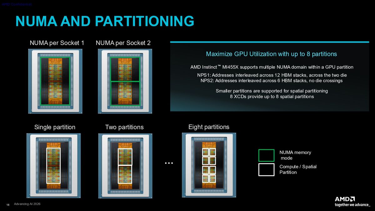
The full MI455X GPU is a massive chip encompassing 320 billion transistors, and it’s built up using advanced packaging technologies. Four Accelerator Complex Dies (XCDs) are stacked on top of each Fabric and Cache Die (FCD) using hybrid bonding. In turn, the two FCDs are each joined to six stacks of HBM4, the two I/O dies, and to one another using TSMC’s CoWoS-L technology.
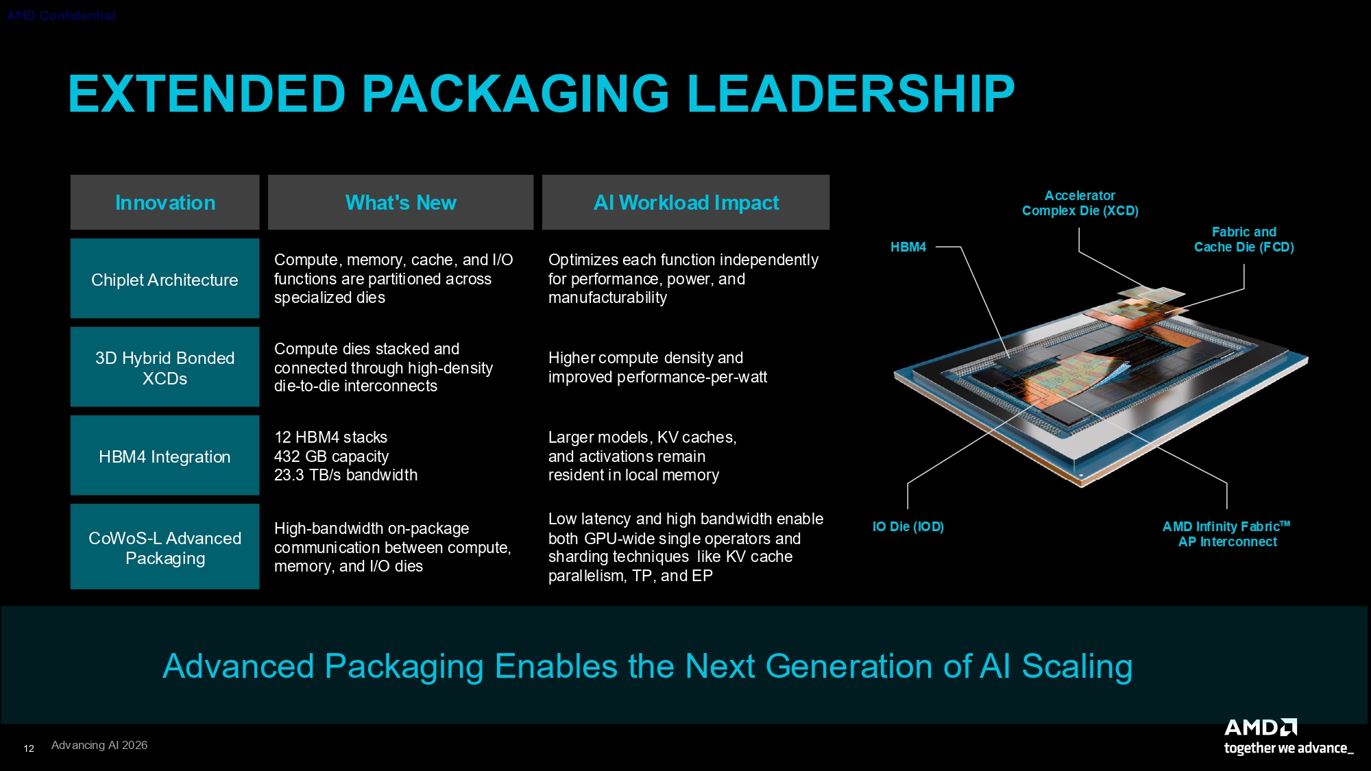
This chiplet design lets AMD use the most advanced TSMC 2N gate-all-around (GAA) process technology on the XCDs, where it’s most beneficial for power and performance, while the FCDs and I/O dies, which contain elements that don’t benefit from the densest process technologies, are fabricated on TSMC N3P.
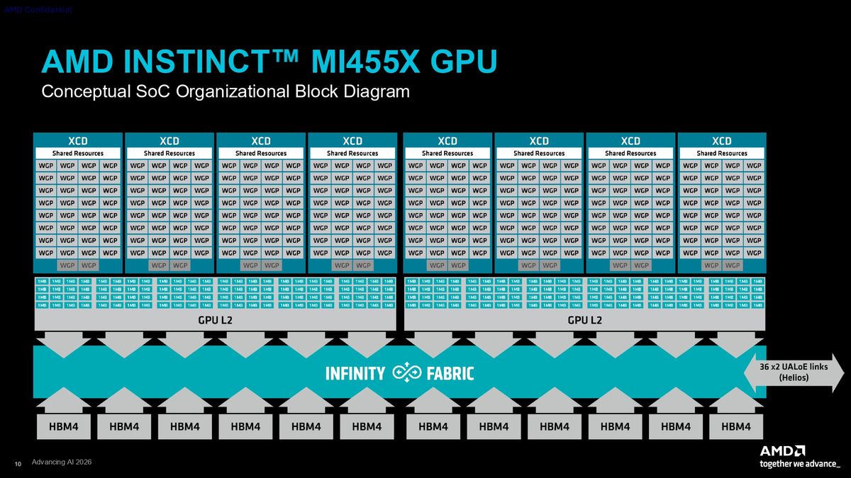
CDNA 5 represents a large shift in the shape of the CDNA architecture. AMD now calls the fundamental building block of the CDNA 5 Accelerator Complex Die a “Work Group Processor” instead of a “Compute Unit,” but in practice, the basic layout of the rest of the Accelerated Complex Die (XCD) is largely similar.
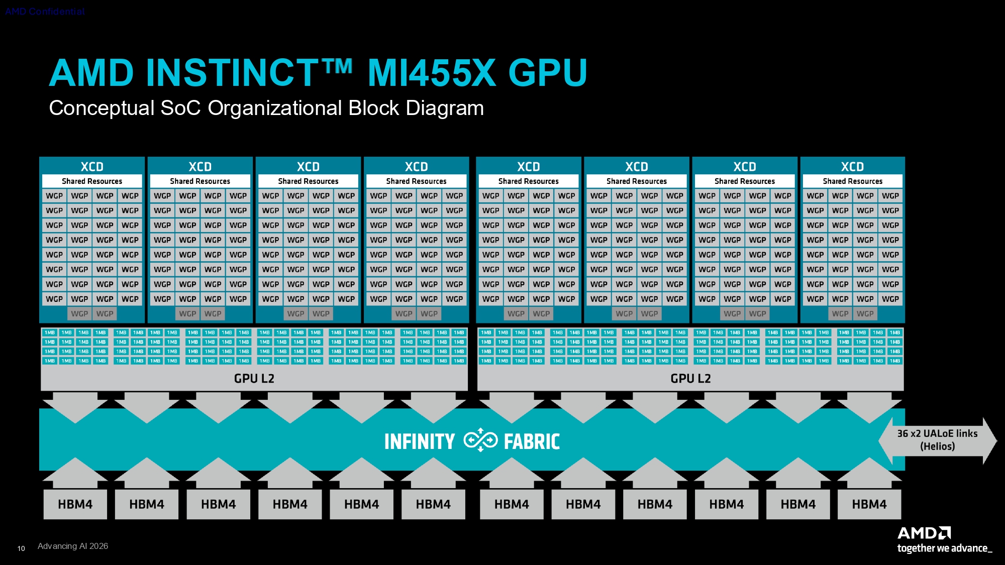
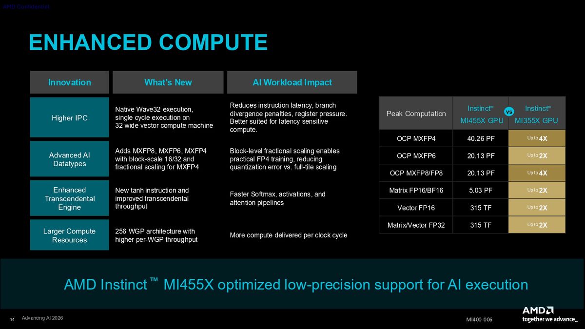
The number of WGPs on the MI455X remains the same as on the MI355X at 256. Because there hasn’t been a change to the number of fundamental compute resources on the chip, the per-WGP throughput on the CDNA 5 MI455X has to be much higher than on the MI355X to deliver its large performance boost.
Among the many other changes for this generation, CDNA 5 marks a major shift for the programming model of an Instinct GPU. The width of a wavefront, or group of work items or threads that each workgroup processor addresses, is now 32 instead of 64, a choice AMD says improves instruction latency, branch divergence penalties, and register pressure. It further explains that a 32-wide approach increases the flexibility of the architecture for interacting with different tensor tile sizes and mapping compute kernels to the hardware. RDNA GPUs have used a native wavefront size of 32 since their introduction.
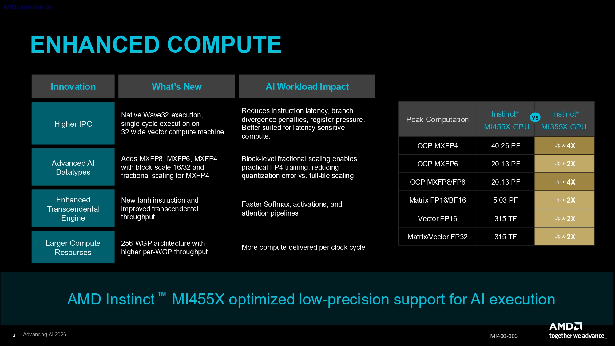
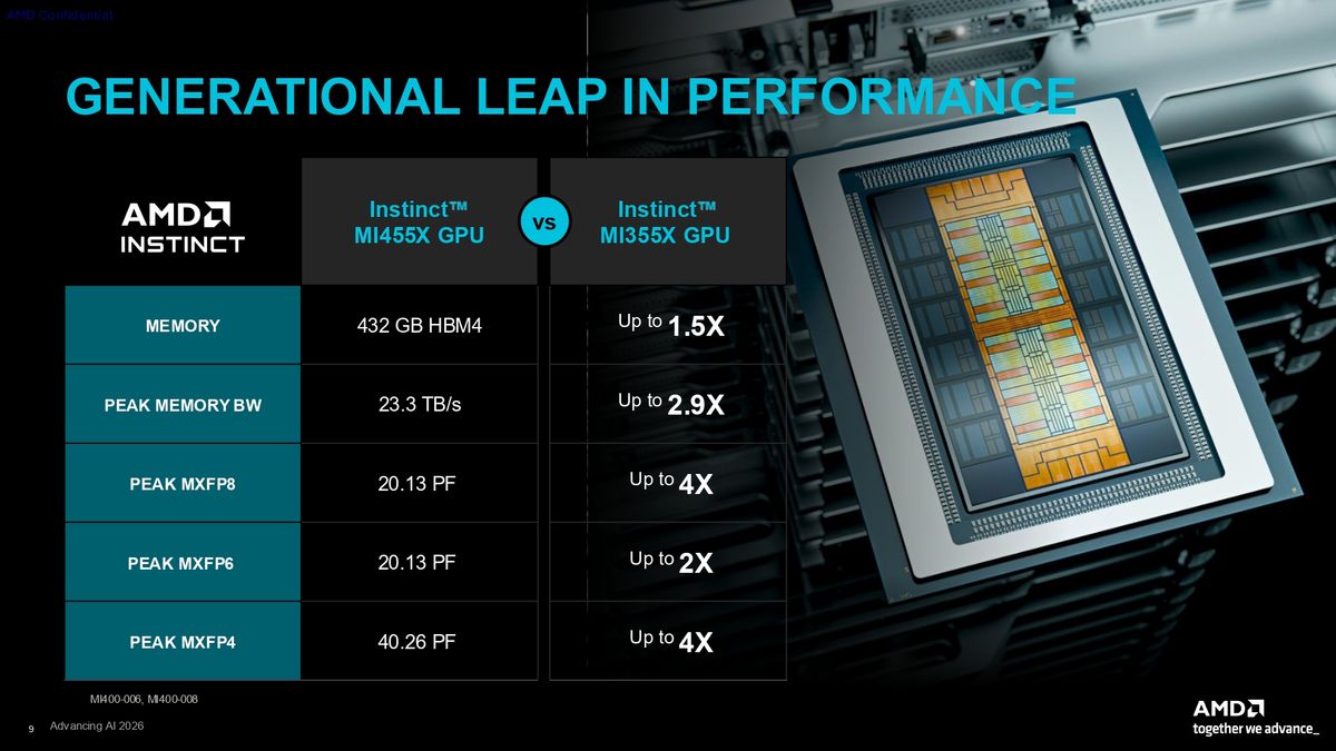
CDNA 5 greatly enhances compute performance over CDNA 4, theoretically doubling and in some cases quadrupling the peak FLOPS possible from the chip. The MI455X especially benefits lower-precision floating-point formats now common for use in inference. OCP MXFP8 and MXFP4 formats are theoretically up to 4X faster than on the CDNA 4 MI355X.
Here’s an overview of the MI455X’s theoretical peak FLOPS compared to both the previous-generation MI355X and Nvidia’s Rubin GPU.
Swipe to scroll horizontally
| Row 0 - Cell 0 | Instinct MI355X |
Instinct MI455X |
Nvidia Rubin |
NVFP4 (dense) |
-- |
-- |
35 PF |
OCP MXFP4 |
10 PF |
40.26 PF |
-- |
OCP MXFP6 |
10 PF |
20.13 PF |
17.5 PF |
OCP MXFP8 |
10 PF |
20.13 PF |
17.5 PF |
Matrix FP16/BF16 |
2.5 PF |
5.03 PF |
4 PF |
Vector FP16 |
157.3 TF |
315 TF |
-- |
Matrix FP32 |
157.3 TF |
315 TF |
400 TF |
Vector FP32 |
157.3 TF |
315 TF |
130 TF |
At least on paper, the MI455X offers peak performance that bests what Nvidia has shown for Rubin so far, and in combination with the Helios rack-scale architecture that finally gives AMD the same 72-GPU coherent domain as Nvidia’s NVL72 rack-scale design, AMD is more competitive in the AI data center capacity race than ever before. And that’s translating into real customer wins, as AMD has announced pivotal deals with Microsoft and Anthropic this week.
But we’d be careful about drawing too many conclusions from these head-to-head peak FLOPS numbers, as the realized performance of these GPUs in the real world is likely to be much lower in practice, as AMD itself admitted in one of our sessions. The ongoing challenge will be to optimize software and applications to achieve as much of that theoretical performance as is possible.
Beyond its general compute improvements, AMD is also touting improved transcendental math performance from the CDNA 5 Transcendental Unit, which has wide-reaching implications for performance on essential AI functions like softmax, neural network activations, and attention. AMD says that the CDNA 5 Transcendental Unit doubles throughput versus CDNA 4. The Transcendental Unit also adds support for an explicit tanh instruction, which is useful for certain operations on hidden layers within neural networks.
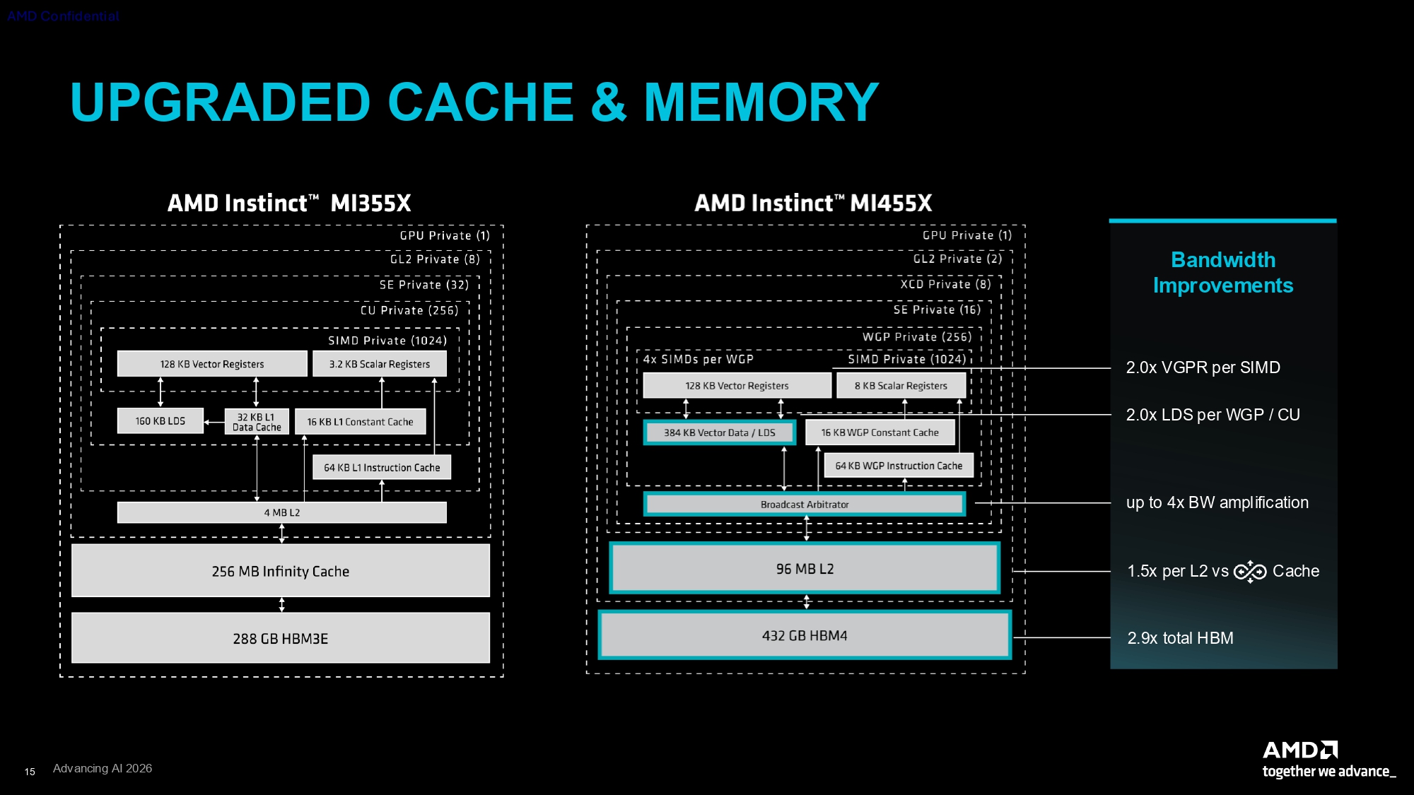
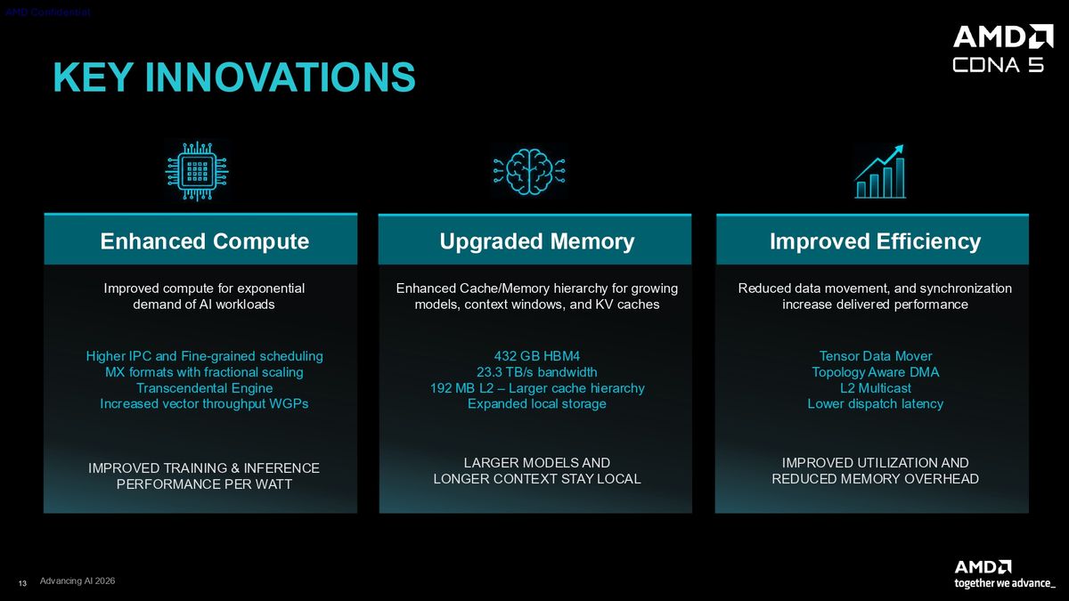
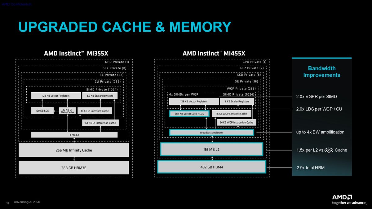
AMD also deeply revised the cache and memory hierarchy on the MI455X. The large Infinity Cache on CDNA 4 has been ditched in favor of a smaller but higher-bandwidth shared L2 cache on each Fabric Compute Die. Each FCD has a 96MB L2 slice for 192MB in total, compared to just 32MB backed by the 256MB Infinity Cache on the MI355X. AMD says this cache offers 1.5X higher bandwidth per FCD compared to the CDNA 4 Infinity Cache, so in aggregate, the MI455X has 3X the L2 bandwidth compared to the MI355X.
Within the WGP, larger, faster, and more flexible caches are now available. The local data store (LDS) or scratchpad memory has doubled in size versus CDNA 4, to 320 KB, and in total, there is 96 MB of LDS across the chip, twice that of the largest CDNA 4 implementation on the MI355X. AMD says the LDS SRAM offers higher read and write bandwidth per clock than in the previous generation, but it didn’t provide specifics.
Critically, the main memory architecture of MI455X has moved to HBM4 for this generation. AMD uses six stacks of HBM4 per FCD for a total of 12 on the chip, offering a memory capacity of 432GB and memory bandwidth of 23.3 TB/s per GPU. High memory capacity and bandwidth are both crucial for keeping ever-expanding AI model weights and KV caches close to the GPU for the best performance.
This HBM implementation is one of the MI455X’s strongest advantages over Nvidia’s Rubin in isolation. It offers both much higher capacity and slightly higher bandwidth than the first Rubin GPU that Nvidia detailed this week. In its initial configuration, Rubin only offers 288GB of HBM4 with up to 22 TB/s of bandwidth.
At rack scale, the MI455X’s higher HBM capacity adds up to 31.1 TB of HBM across 72 GPUs, or a whopping 50% more than the 20.7 TB aggregate capacity of Vera Rubin. And the Helios rack-scale architecture is AMD’s first to join all of that GPU memory into a single coherent domain. Since AI inference performance is dominated by both data locality and memory bandwidth, AMD’s advantages in this regard are sure to attract plenty of attention.
Image 1 of 2
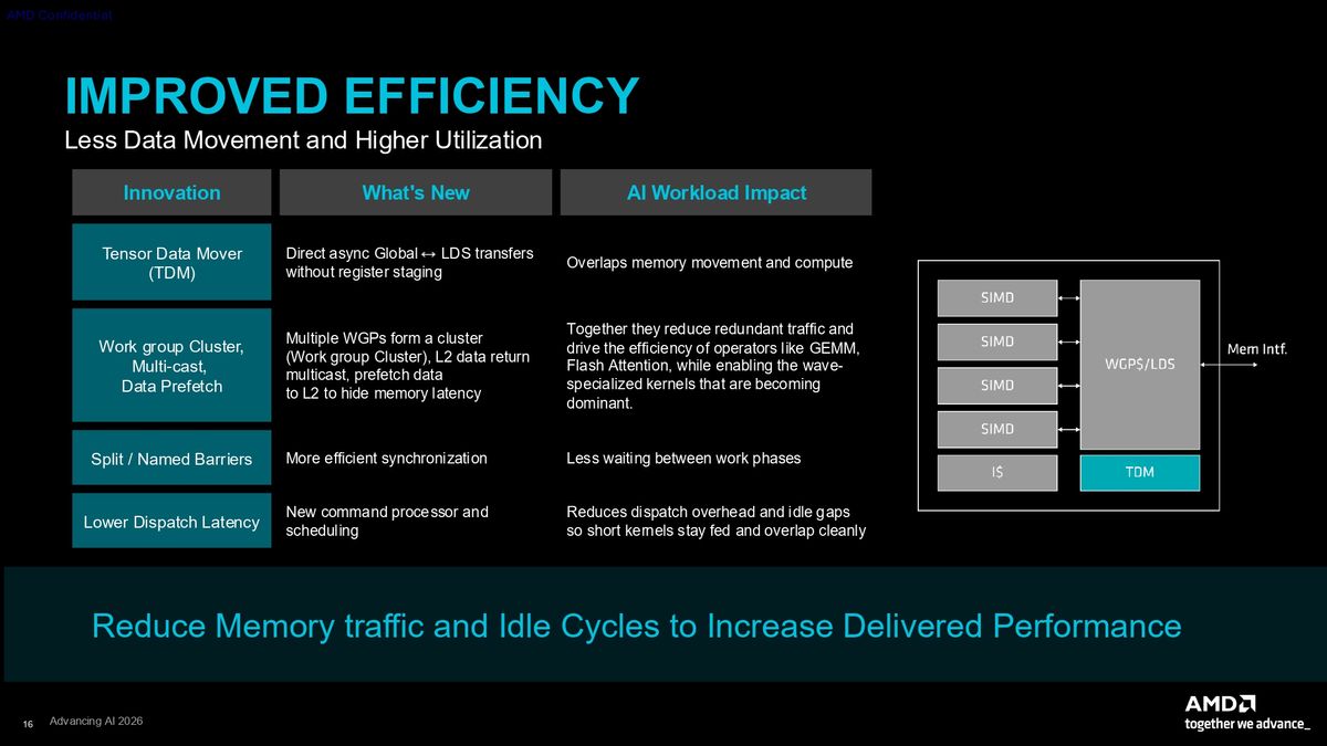
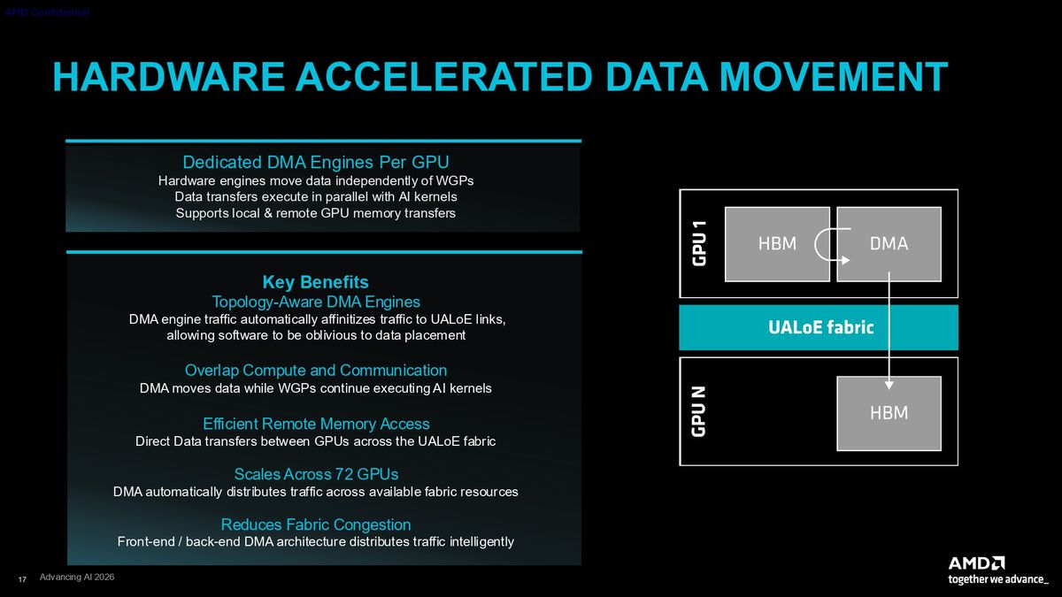
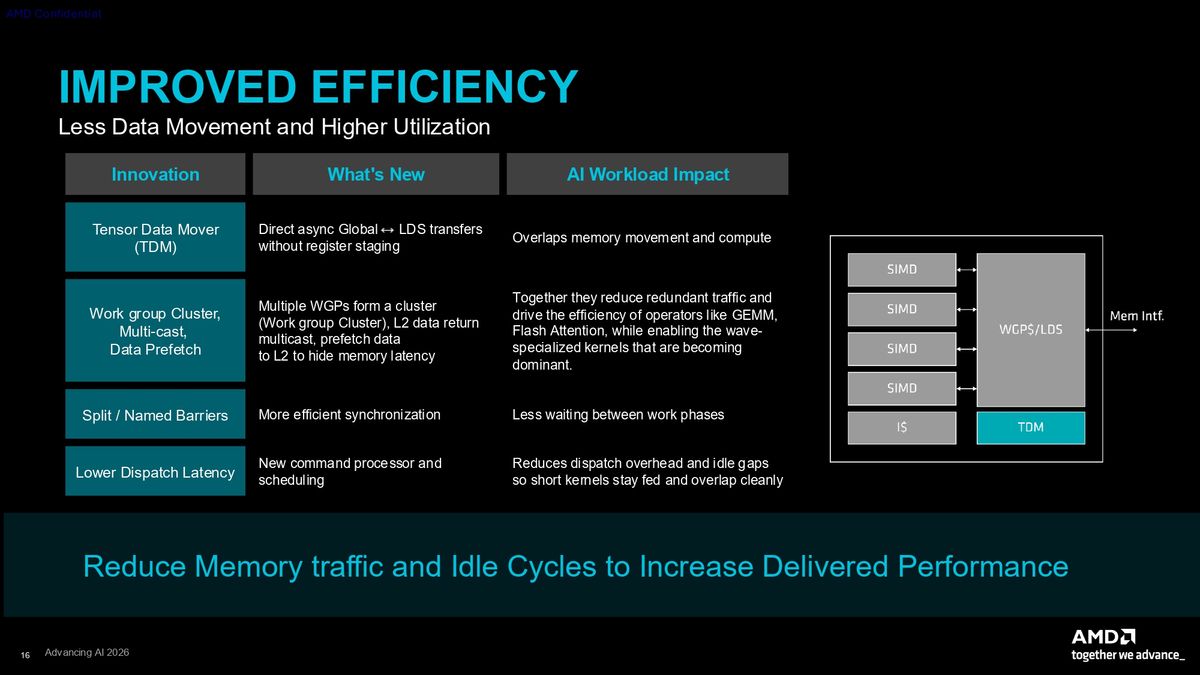
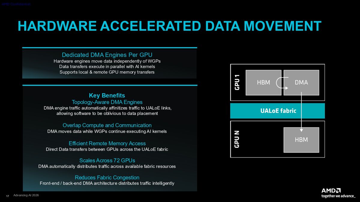
Efficient data movement across the chip is a key consideration for reducing power consumption and improving performance on the MI455X.
The CDNA 5 Tensor Data Mover is an improved version of the data movement engine in past CDNA generations. Like Nvidia’s Tensor Memory Accelerator, the TDM accelerates the production of certain tensor-specific memory addresses and facilitates moving the related data from memory without involving the shader engines. In the CDNA 5 generation, the TDM gains the ability to move data directly from DRAM to the WGP LDS cache without staging data at intermediate cache levels.
AMD has also added multicast support for memory reads to the WGPs to take advantage of the fact that AI workloads often need to work on the same weights and activations across multiple WGPs at once. By using multicast, a single memory read can be amplified across many WGPs, increasing effective memory bandwidth, reducing duplicated traffic on the bus, and lowering power consumption. Nvidia has had a similar capability in its GPUs since Hopper, but given AMD’s intense focus on efficient data movement this generation, it’s perhaps unsurprising to see a version of it added here.
All told, the MI455X is AMD’s most compelling Instinct product yet. It delivers a massive generational performance improvement, it puts up peak FLOPS on paper that are competitive with or even superior to Nvidia’s upcoming Rubin GPU, and it offers a massive 432GB pool of HBM4 memory that’s 1.5x larger and even slightly faster than Rubin’s 288GB complement.
Combined with the Helios rack-scale architecture and its 72-accelerator scale-up domain—AMD’s first true answer to Nvidia’s NVL72 rack-scale design—we should expect the race for AI compute superiority to really heat up in the second half of this year as both Nvidia and AMD begin delivering their next-generation products to customers.
Image 1 of 17

Follow Tom's Hardware on Google News, or add us as a preferred source, to get our latest news, analysis, & reviews in your feeds.







 English (US) ·