
 3 hours ago
7
3 hours ago
7
Could Nvidia's days of datacenter dominance be threatened? With the launch of Helios, AMD’s first true rack-scale AI platform, the House of Zen is done playing catch up.
The company claims the rack system is powered by the fastest AI accelerators on the market. And, at least on paper, the 72-GPU system is not only bigger and faster by nearly every metric than Nvidia’s existing Blackwell-based rack systems but than Vera Rubin as well, and that includes the rack.
Measuring in at 1.2 meters wide and 44OUs high, the OCP Open Rack Wide form factor is nearly twice the size of Nvidia's NVL72, and AMD has clearly put the extra space to good use.
Compared to Vera Rubin, Helios boasts 50 percent more HBM4 and scale out bandwidth and between 15 and 25 percent higher performance for AI training.
Vera Rubin’s adaptive compression tech will supposedly give it a 25 percent lead over Helios at FP4, but, as we understand it, that’s only for inference workloads. For applications that can’t, Helios offers 15 percent higher peak FP4 FLOPS.
To be clear, it’s not the first time we’ve seen AMD pull ahead on memory or FLOPS. The difference is those products usually launched a year after Nvidia’s equivalent part. Helios launches right in time with Nvidia’s Vera Rubin platform.
AMD estimates Helios' higher peak performance will give it a 30 percent performance per dollar lead over the competition.
The belly of the beast
Helios' performance gains are rooted in an all-new GPU built on AMD’s 5th-gen CDNA compute architecture.
Much like the rack it powers, the Instinct MI455X is massive, though the chip is underselling it a bit. Just like the MI300 series, AMD’s latest datacenter GPU is a silicon sandwich that stitches together I/O, compute, and memory in a single package.

Like previous Instinct GPUs, the MI455X isn't one chip, but nearly two dozen compute, I/O, and memory chiplets stitched together with TSMC's advanced packaging tech. Image credit AMD
Including memory, MI455X features 24 chiplets using a combination of 2.5D and 3D packaging technologies. The chip’s eight compute dies are fabbed on TSMC’s bleeding edge 2nm process tech, which are stacked atop a pair of 3nm fabric and cache dies (FCDs). The FCDs are an interesting twist on the formula. They function as a cache heavy interposer with 96 MB of L2 cache each and the memory controllers for the chip’s 12, 36 GB HBM4 stacks.
Unlike past Instinct accelerators in which the I/O die was located under the compute, the MI455X breaks these out into two new dies — also fabbed on TSMC’s 3 nm — which are responsible for chip-to-chip communication.

AMD's chiplet architecture means it can function as one big GPU, two smaller ones, or up to eight virtualized accelerators. Image credit AMD
One benefit to this architecture is that the chip can be made to function as one big GPU or two smaller ones depending on which NUMA configuration you opt for. The chip also supports spatial partitioning into up to eight virtual GPUs.
Under the hood, AMD’s CDNA architecture brings some notable improvements over the last generation. Compared to last year’s MI355X, the MI455X promises as much as 4x higher floating point performance for AI workloads.

In just a year, AMD has managed to deliver a 4x uplift in floating point performance over MI355X. Image credit AMD
Most notably, the MI455X forgoes FP64 entirely in order to dedicate as much die area to AI-centric datatypes like MXFP4 and MXFP8 as possible. This generation also adds support for 16 and 32 block scale data types. For those needing FP64 compute, that functionality will be served by a different HPC centric SKU.
This isn’t the only physical change. As we mentioned earlier, for this generation, AMD has opted for a larger shared L2 cache and ditched its last level “Infinity” cache altogether.
The benefit, AMD fellow Alan Smith says, is higher bandwidth and a simplified data path compared to last gen. “The bandwidth delivered for one of these L2 caches in MI455X is 1.5x the aggregate bandwidth of the Infinity cache on MI355X."
Along with prioritizing low precision compute, AMD configured the chip’s execution engines to boost IPC and implemented a new direct memory access (DMA) engine to minimize data movement.
Racking it up
While bigger than Nvidia’s NVL72, AMD’s Helios rack architecture is remarkably similar.
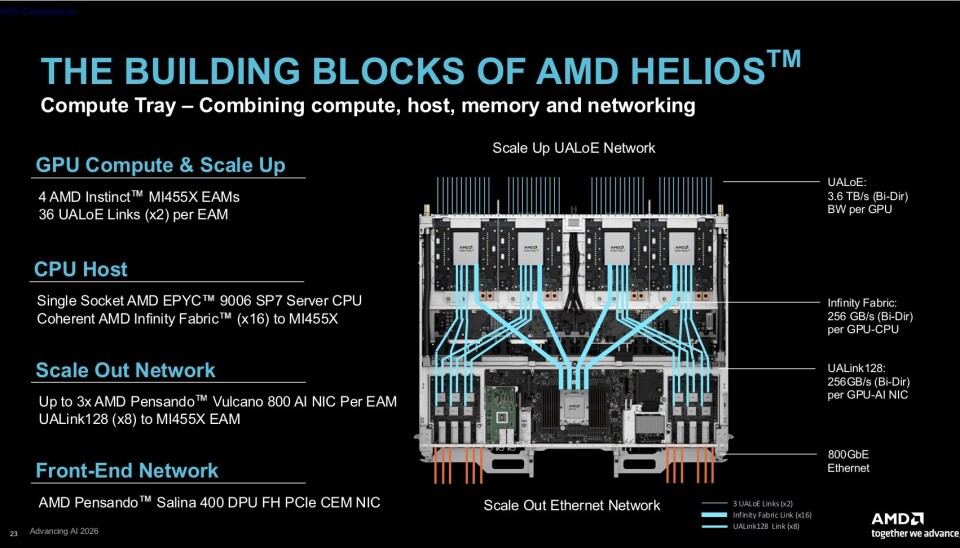
Here's a quick rundown of the Helios compute blade, which crams four MI455X GPUs, 12 Vulcano smartNICs, a Salina DPU, and a 96-core Venice Epyc CPU into a 1OU form factor. Image credit AMD
Both systems pack 72 GPUs spread across 18 liquid-cooled compute blades. Each blade is equipped with four MI455Xs, but rather than two CPUs per blade like you’d find on NVL72, AMD has opted for a single 96-core Venice Epyc clocking up to 5 GHz, though OEMs and hyperscalers could theoretically spec each blade with up to 256 cores, if they wanted to.

Each of Helios' 6 switch blades features two 102.4 Tbps Broadcom Tomahawk 6 switch ASICs. Image credit AMD
The scale-up fabric used to make the six dozen GPUs behave as one great big one is, it shouldn't surprise anyone, also quite similar to Nvidia's NVL72. But rather than NVLink, AMD is tunneling Ultra Accelerator Link over Ethernet (UALoE).
This means AMD doesn’t need bespoke switches and system builders can get away with merchant silicon from the likes of Broadcom — and that’s exactly what they’ve done.
The Helios reference design uses 12 of Broadcom’s 102.4 Tbps Tomahawk 6 switch ASICs spread across six switch trays. Each provides 512 lanes of 200 Gbps connectivity, just enough to feed each MI455X with 3.6 TB/s of bidirectional bandwidth.

The all-to-all scale up fabric ensures that any one GPU can talk to any other while keeping latency to an absolute minimum. Image credit AMD
Helios’ scale out networking is also quite a bit beefier than Nvidia’s Vera Rubin. The Nvidia platform pairs each GPU with a single 1.6 Tbps ConnectX-9 superNIC. By comparison, each MI455X gets three of AMD’s 800 Gbps Pensando Vulcano network cards for a total of 2.4 Tbps of scale out bandwidth per accelerator.
These scale out NICs are designed for large scale inference and training workloads that require multiple racks' worth of GPUs. For front-end communications, which include management, API traffic, and storage, each of Helios' 18 compute blades is equipped with a 400 Gbps Pensando Salina data processing unit (DPU).

Here's an exploded view of the Helios rack showing all of the supporting infrastructure, like cable carts, coolant manifolds, and power delivery necessary to keep the system humming along. Image credit AMD
All of this is powered by a 50 volt liquid-cooled DC bus bar located at the back of the system that under load can deliver between 225 and 245 kW of power. Nvidia hasn’t shared system-level power consumption for its Vera Rubin racks just yet, but our best estimates put peak power consumption at somewhere between 240 and 250 kW.
If Helios can deliver the performance claimed and our power estimates are accurate, that would not only make the platform faster than Vera Rubin, but more power efficient as well.
There are FLOPS and then there are achievable FLOPS
Unfortunately for AMD, Helios realistically won’t touch 40 petaFLOPS in the real world, but then again Nvidia probably won’t hit its claimed FLOPS figures for the same reasons.
Peak theoretical FLOPS are a mathematical approximation derived from OPS per clock cycle per unit of compute at a given frequency. The problem is modern accelerators don’t run at a fixed clock. They follow boost curves tied to available power and thermals, and even with liquid cooling, these things get hot.
And that’s before we take into consideration the workloads and the software used to run them. AI is dominated by matrix multiplication, and if the matrix isn’t the right shape, the max achievable matmul FLOPS (MAMF) won’t get anywhere close to peak. Poorly optimized GPU kernels or compute libraries only compound this issue, and no software is perfect.
What this means in practice is that the FLOPS you see advertised on these systems’ spec sheets and marketing are really a ceiling, one that in the real world is functionally impossible to reach.
AMD knows this and has quietly begun tweaking its marketing to focus more on measured performance than the theoretical. We saw this with the recently unveiled MI355X, where the company listed both peak and achieved FLOPS and with Helios.

It's an open secret in accelerated computing that achievable FLOPS rarely come close to the number on the spec sheet. Image credit AMD
Speaking with the press ahead of Thursday’s keynote, Anush Elangovan, VP of AI software at AMD, boasted that in real world testing, MI455X achieved 20 petaFLOPS of FP4 performance — half of peak.
Whose roofline is higher is still a useful metric, but the more meaningful, albeit difficult to pin down, is who gets closer to it.
So while 50 percent of peak performance may not sound very good, Elangovan remains confident that the MI455X still delivers higher performance than any accelerator on the market.
“It's delivered bandwidth and flops, and it is still the best in the industry today. There is no other accelerator that I have seen that can hit that yet,“ he said.
AMD’s candidness around real world performance hasn’t dissuaded the major model builders and hyperscalers. The House of Zen now counts Meta, Microsoft, and Oracle as customers. Meanwhile, OpenAI has committed to deploying gigawatts of MI455X GPUs, in exchange for a roughly 10 percent stake in the chipmaker. Similarly Anthropic plans to deploy two gigawatts of the chips in exchange for an up to $5 billion investment in the model dev.
Much more to come
Helios may be AMD’s flagship GPU platform, but the company recognizes that not everyone is ready for a 225-plus kW rack. Alongside the MI455X, AMD is working on several other CDNA 5-based GPUs including one optimized for enterprise deployments.

AMD's MI400 series GPUs will span three configurations from hyperscale and enterprise AI to mixed AI and HPC. Image credit AMD
First teased at CES last winter, the MI440X is a cut down version of the MI455X that will be offered in a more traditional eight GPU form factor.
Meanwhile for those less concerned with AI and more interested in high-performance computing, AMD is also working on a specialized version of the chip, called the MI430X, that swaps the machine learning-optimized compute dies for ones designed to maximize single (FP32) and double (FP64) precision performance.
These data types are essential for a wide range of high-performance computing (HPC) and scientific computing taking place in research centers and national labs around the globe.
Each chip is expected to deliver north of 200 teraFLOPS, making it the most potent supercomputing accelerator AMD has ever built. And, notably, AMD claims that unlike Nvidia, the chip won’t need FP64 emulation to be competitive.
While details are thin, the MI430X has already won AMD two high profile contracts including EuroHPC’s Alice Recoque supercomputer and Oak Ridge National Laboratory's next-gen Discovery system, which are expected to come online in 2027 and 2028 respectively.
A long and winding road to Venice
Then there are AMD’s sixth-gen Venice Epycs. At Advancing AI this week, we caught a glimpse of AMD’s full datacenter CPU lineup, which will be rolling out over the next year and a half.

AMD says its 6th Gen Epyc Venice SP7 platform is in production, with SP8 and Venice X slated to arrive next year. Image credit AMD
For this generation, AMD has opted for two separate sockets. SP7, which is what AMD is using in Helios and the only Venice CPUs shipping before the end of the year, will support up to 256 cores and 512 threads in a 600 watt socket.
Like AMD’s earlier Genoa generation, AMD will also support a version of the chip aimed at HPC applications that uses its 3D V-Cache tech to boost L3 cache to more than a gigabyte, but these won’t arrive until late next year.
For lower-power enterprise applications, AMD’s SP8-based Venice CPUs, due out in the first half of next year, will offer more modest core counts ranging from eight to 128 in a lower power package. Meanwhile for AI head nodes, AMD is working on a custom version of Venice called Verano that promises 5 GHz boost clocks along with LPDDR5x memory when it arrives late next year. ®






 English (US) ·