
 5 months ago
63
5 months ago
63
AMD unveiled its new MI350X and MI355X GPUs for AI workloads here at its Advancing AI 2025 event in San Jose, California, claiming the new accelerators offer a 3X performance boost over the prior-gen MI300X, positioning the company to improve its competitive footing against its market-leading rival, Nvidia. AMD claims it beats Nvidia in like-for-like inference benchmarks by up to 1.3X and leads by up to 1.13X in select training workloads.
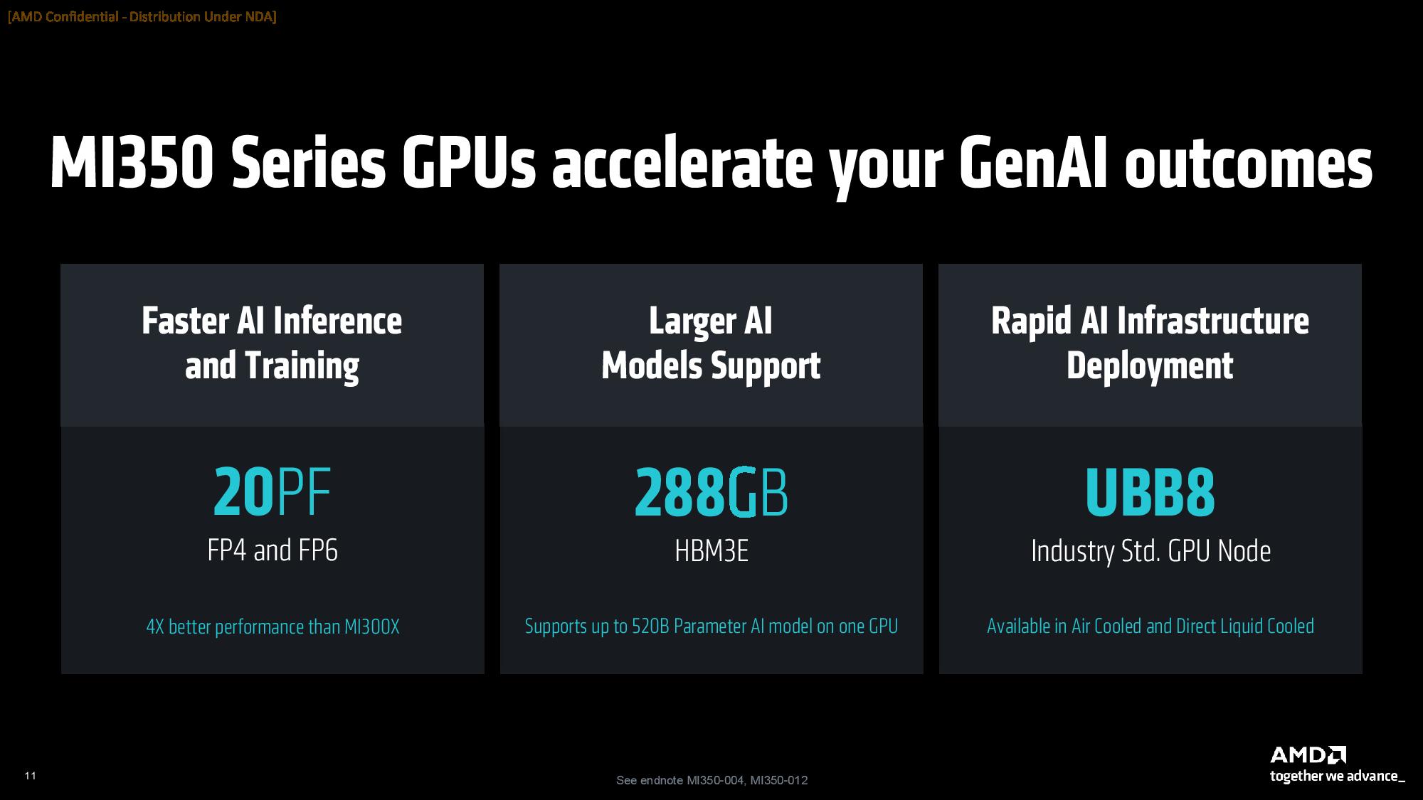
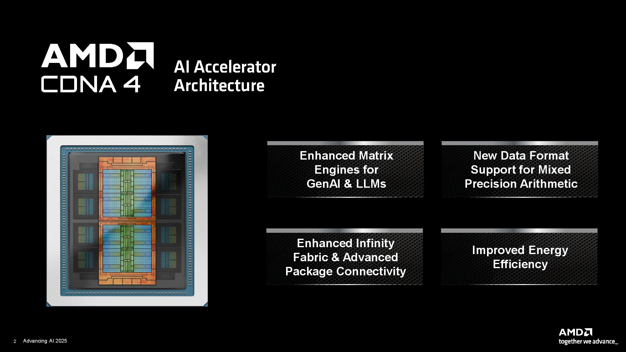
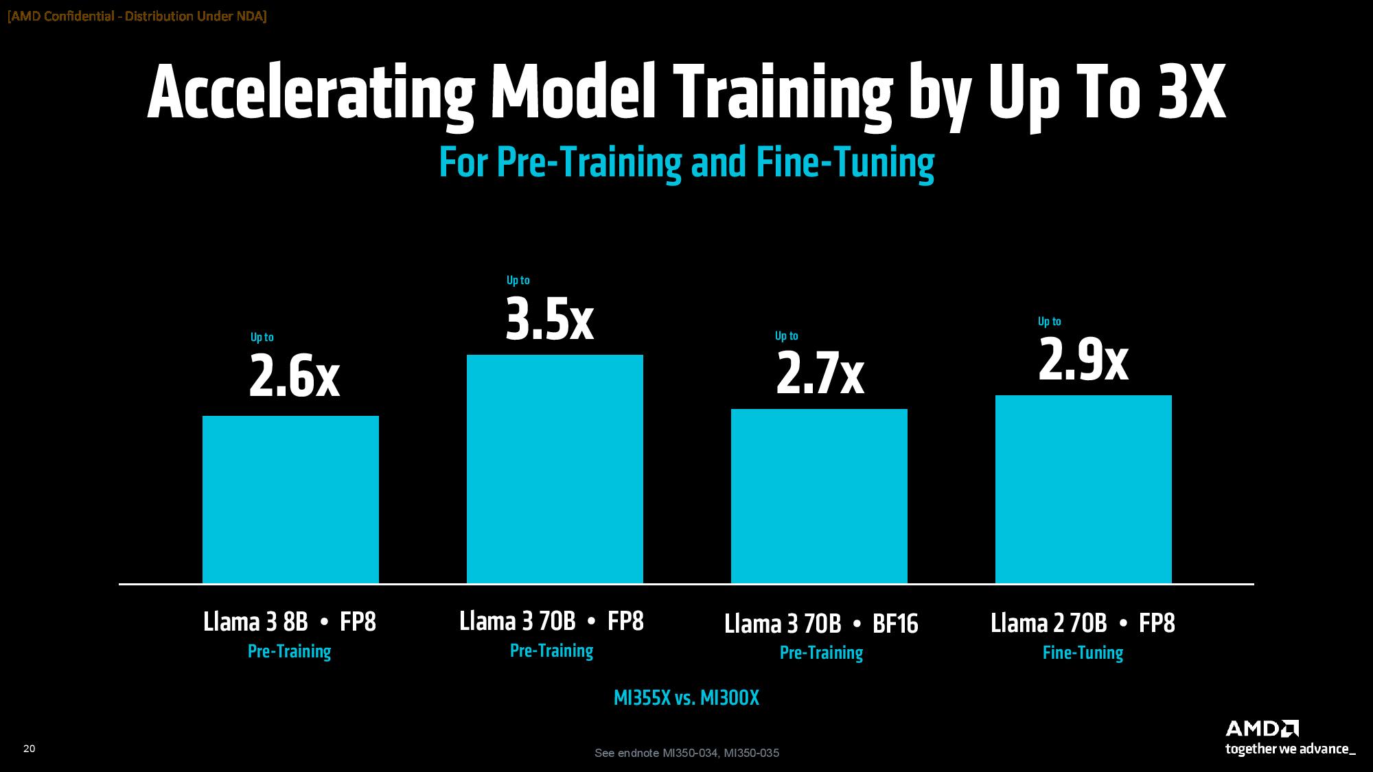
AMD also claims a 4X increase in "AI compute performance" compared to prior-generation AMD MI300X models and a 35X increase in inference performance, largely achieved by transitioning to the CDNA 4 architecture and utilizing a smaller, more advanced process node for the compute chiplets. AMD's production MI350 platforms began shipping last month.
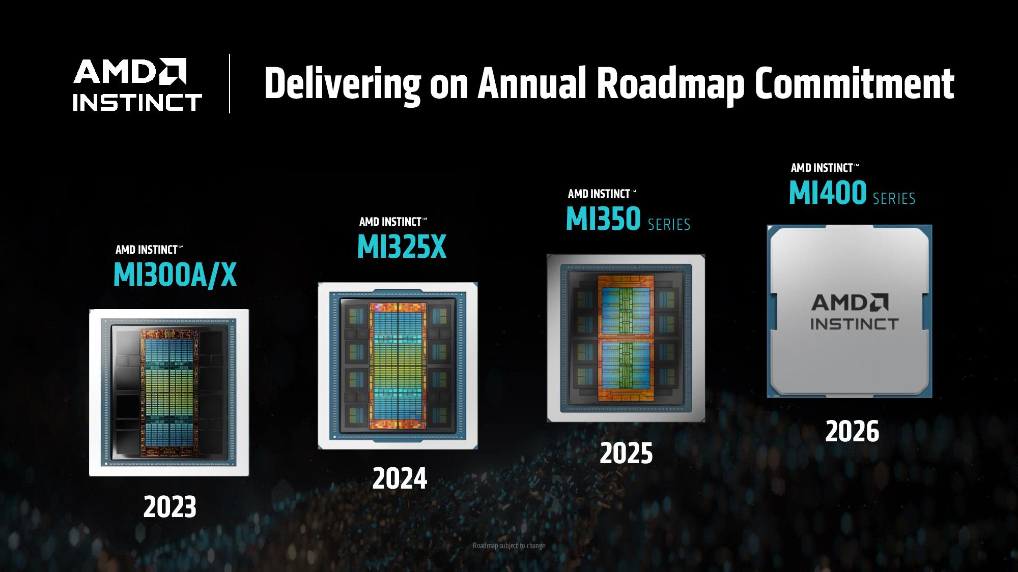
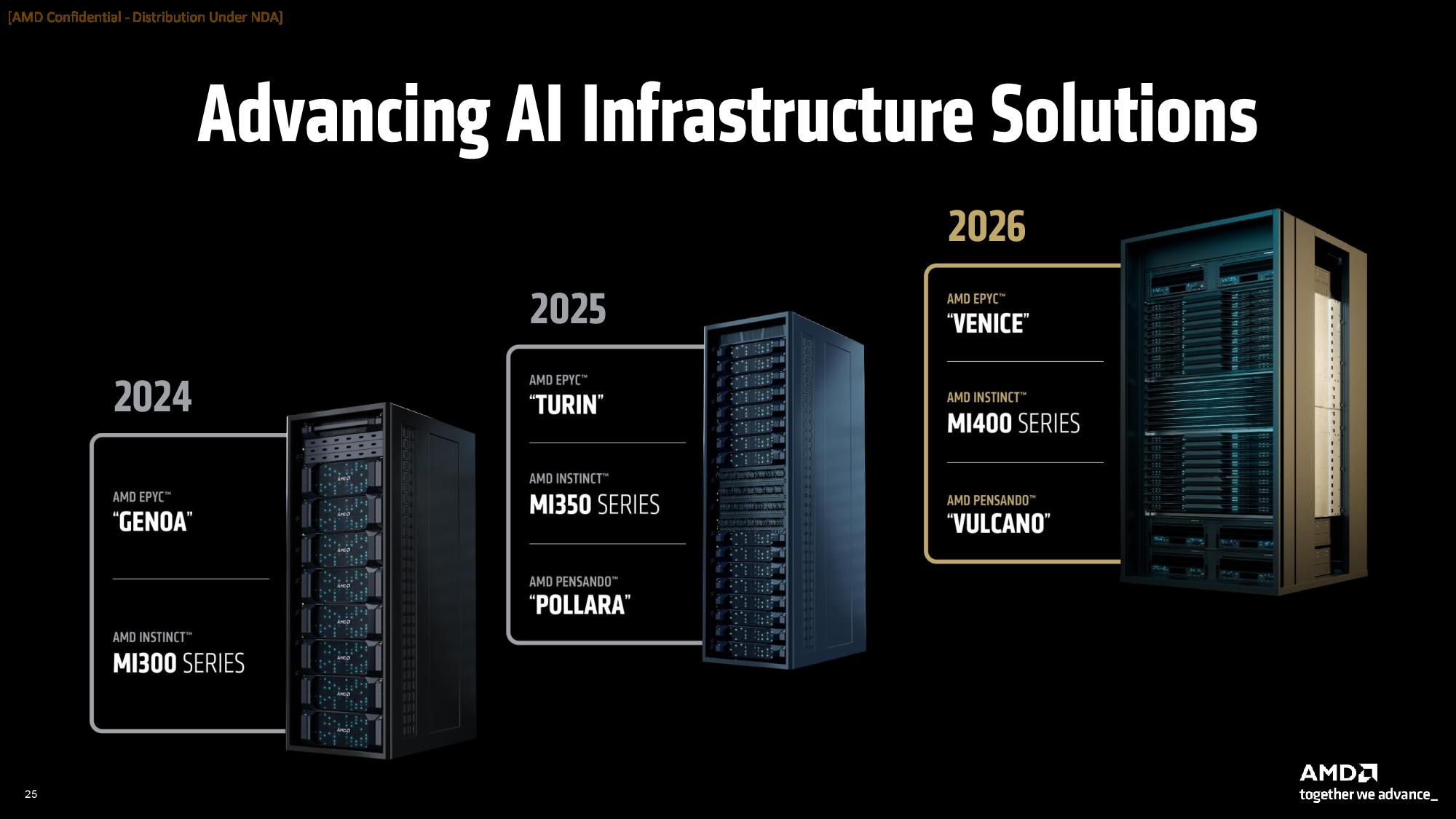
These two MI300 Series AI GPUs will power AMD rack-level solutions for the remainder of the year and into 2026 as the company builds to its MI400 rollout.
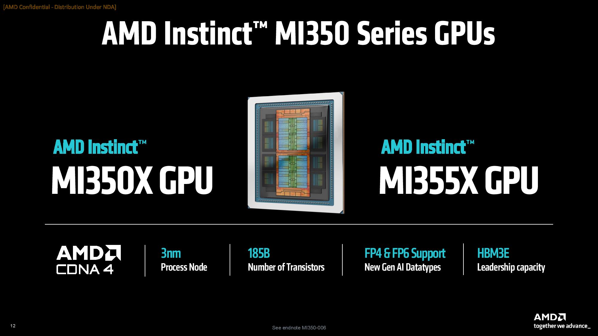
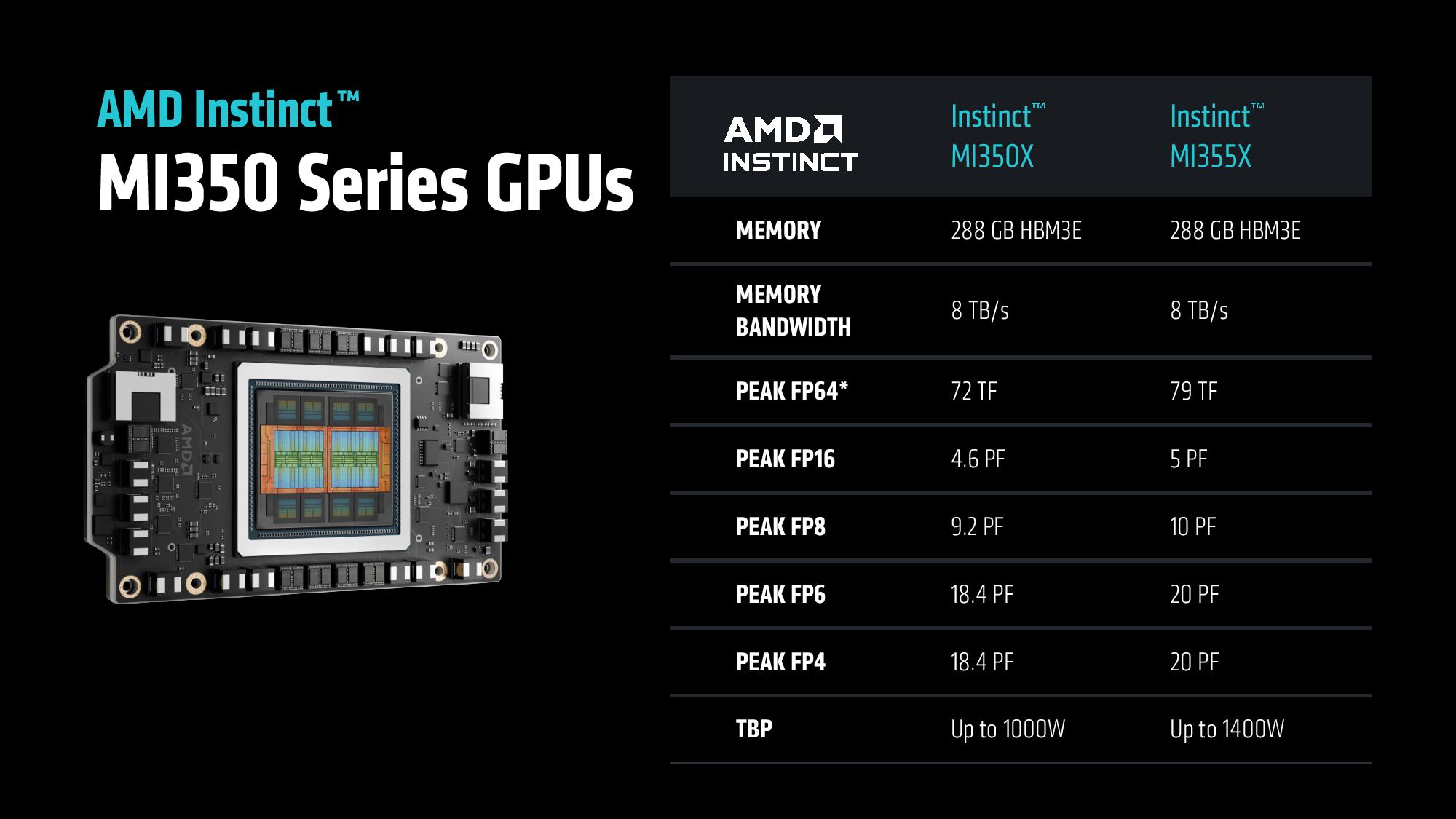
The MI350X and MI355X share an identical underlying design, featuring up to 288GB of HBM3E memory, up to 8 TB/s of memory bandwidth, and new support for the FP4 and FP6 data types. However, the MI350X is geared for air-cooled solutions with a lower Total Board Power (TBP), while the MI355X pushes power consumption up a notch for liquid-cooled systems geared for the highest performance possible.
Swipe to scroll horizontally
GPUs | Instinct MI325X OAM | Instinct MI350X OAM | 8 x Instinct MI350X OAM | Instinct MI355X OAM | 8 x Instinct MI355X OAM |
GPU Architecture | CDNA 3 | CDNA 4 | CDNA 4 | CDNA 4 | CDNA 4 |
Dedicated Memory Size | 256 GB HBM3E | 288 GB HBM3E | 2.3 TB HBM3E | 288 GB HBM3E | 2.3 TB HBM3E |
Memory Bandwidth | 6 TB/s | 8 TB/s | 8 TB/s per OAM | 8 TB/s | 8 TB/s per OAM |
| FP64 Performance | Row 4 - Cell 1 | 72 TFLOPs | 577 TFLOPs | 78.6 TFLOPS | 628.8 TFLOPs |
| FP16 Performance | 2.61 PFLOPS | 4.6 PFLOPS | 36.8 PFLOPS | 5 PFLOPS | 40.2 PFLOPS |
| FP8 Performance | 5.22 PFLOPS | 9.2 PFLOPs | 73.82 PFLOPs | 10.1 PFLOPs | 80.5 PFLOPs |
| FP6 Performance | Row 7 - Cell 1 | 18.45 PFLOPS | 147.6 PFLOPS | 20.1 PFLOPS | 161 PFLOPS |
| FP4 Performance* | Row 8 - Cell 1 | 18.45 PFLOPS | 147.6 PFLOPS | 20.1 PFLOPS | 161 PFLOPS |
AMD will not release an APU version of this chip like it did with last generation's MI300A, which featured both CPU and GPU cores on a single die. In contrast, this generation will have GPU-only designs.
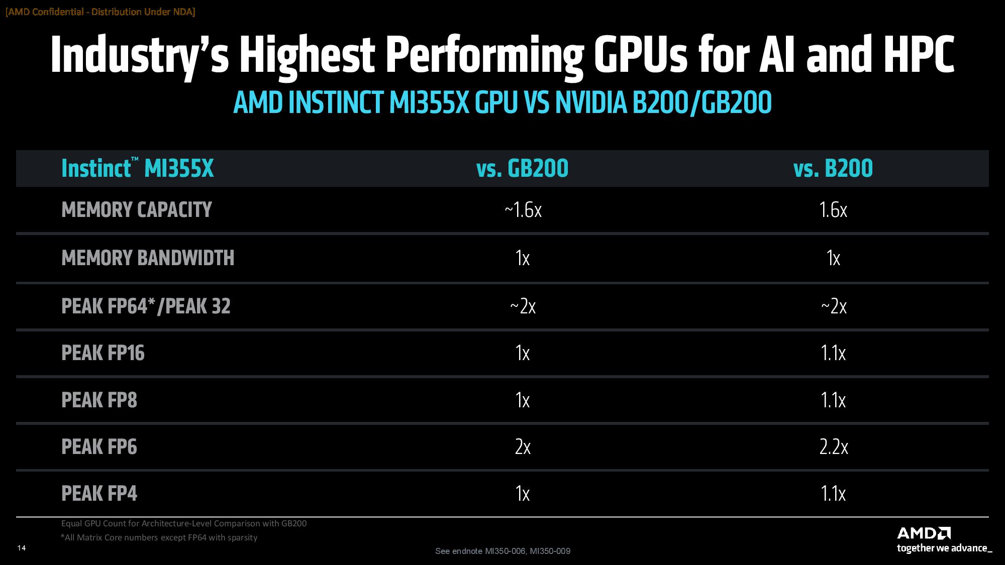
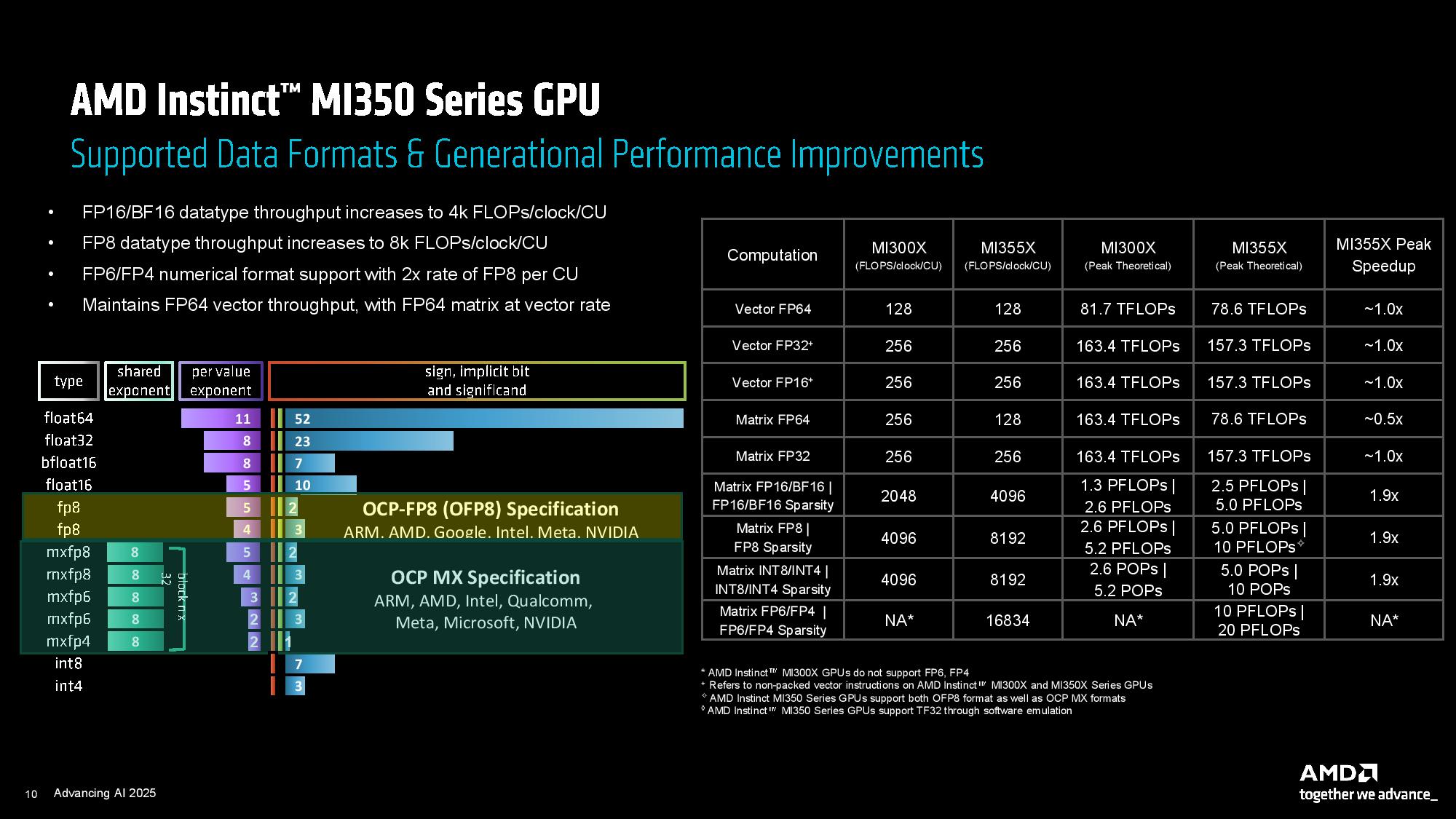
AMD's MI355X comes with 1.6 times the HBM3E memory capacity of Nvidia's competing GB200 and B200 GPUs, but delivers the same 8TB/s of memory bandwidth. AMD claims a 2X advantage in peak FP64 / FP32 over Nvidia's chips, which isn't surprising given Nvidia's optimization focus on the more AI-friendly lower-precision formats. Notably, MI350's FP64 matrix performance has been halved compared to MI300X, though vector performance drops by roughly 4% gen-over-gen.
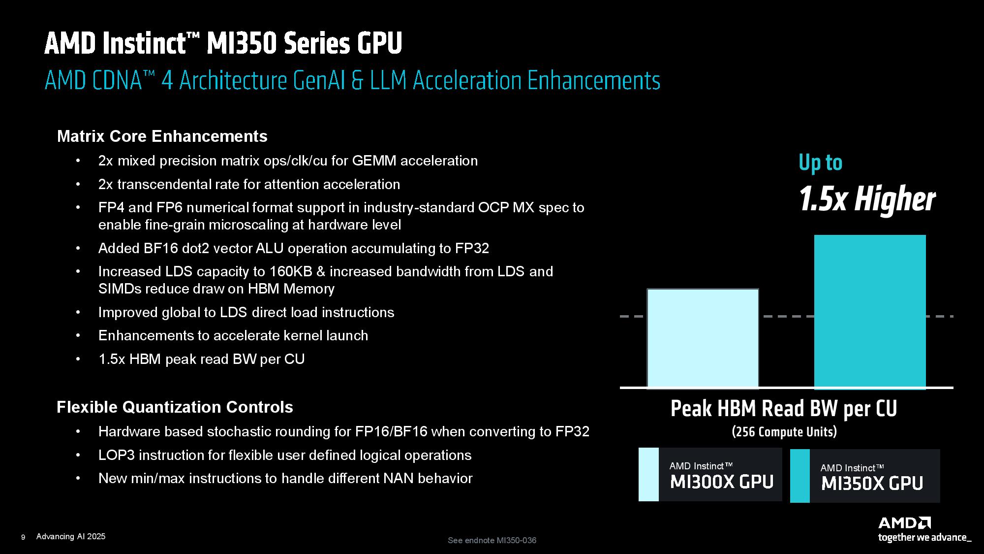
As we move down to lower-precision formats, such as FP16, FP8, and FP4, you can see that AMD generally matches or slightly exceeds the Nvidia comparables. One notable standout is FP6 performance, which runs at FP4 rates, which AMD sees as a differentiating feature.
As we've also seen with Nvidia's competing chips, the new design and heightened performance also come with increased power consumption, which tops out at a 1,400W Total Board Power (TBP) for the liquid-cooled high-performance MI355X model. That's a marked increase from the MI300X's 750W and the MI325X's 1,000W thermal envelopes.
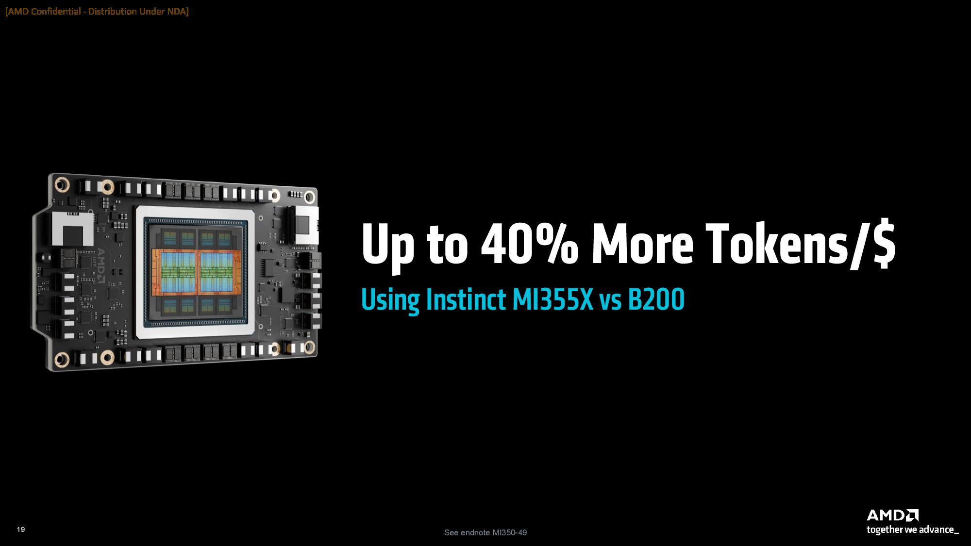
AMD says this increase in performance density allows its customers to cram more performance into a single rack, thereby decreasing the all-important performance-per-TCO (total cost of ownership) metric, which quantifies performance-per-dollar at the rack level.
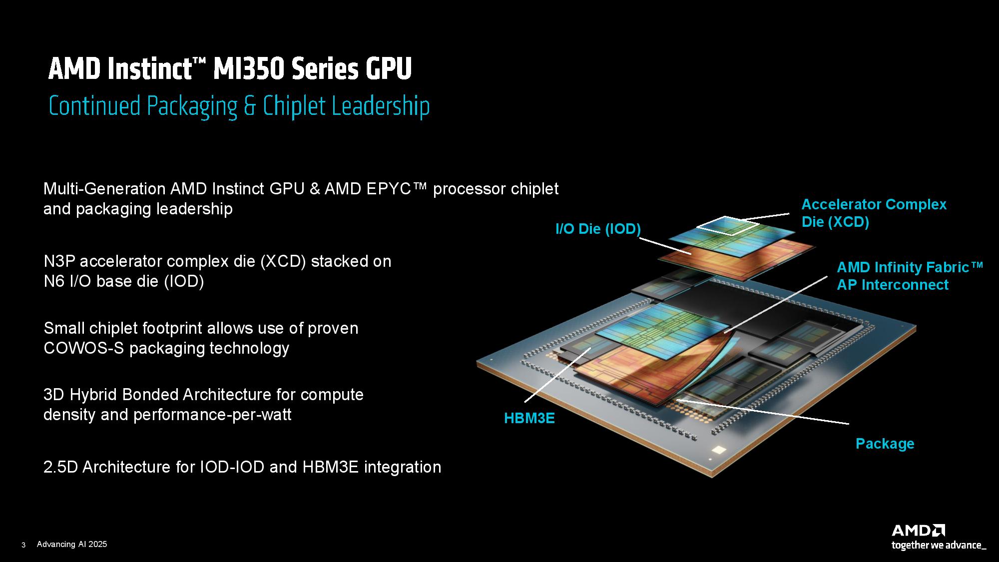
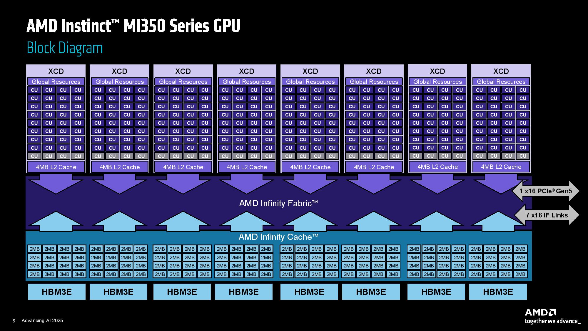
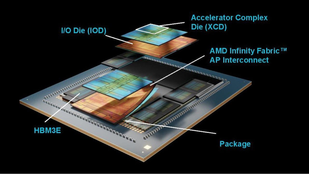
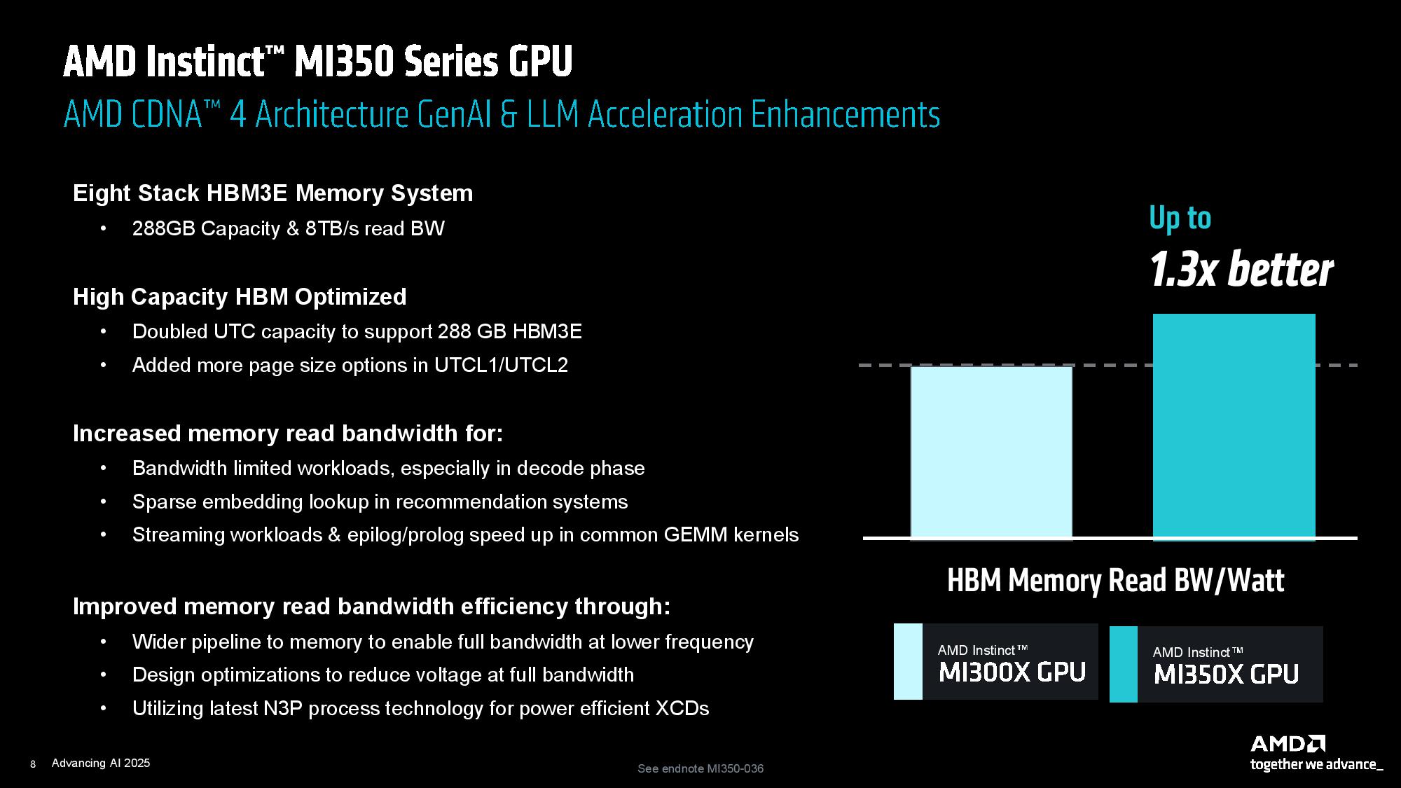
The new chips feature numerous advancements in performance, but the fundamental design principles of merging 3D and 2.5D packaging technology remain unchanged, with the former being used to fuse the Accelerator Compute Dies (XCD) with the I/O Dies (IOD), while the latter is used to connect the IOD to each other and the 12-Hi HBM3E stacks.
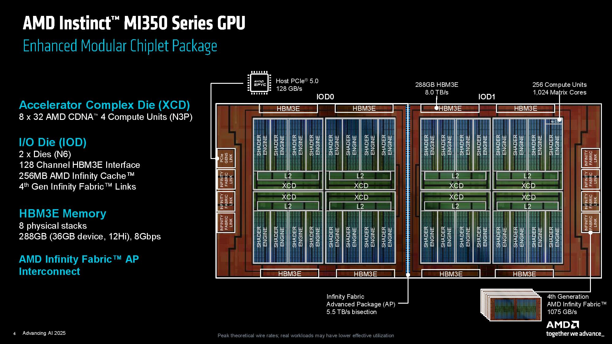
The chip features eight total XCD chiplets, each with 32 compute units (CU) enabled, for a total of 256 CU (AMD has four CU in reserve per XCD to improve yield; these are disabled as needed). The XCD's transition from 5nm with the prior generation to dies fabbed on TSMC's N3P process node for the MI350 series. The total chip weilds a whopping 185 billion transistors, a 21% increase in the transistor budget over the prior generation's 153 billion.
Additionally, while the I/O Die (IOD) remains on the N6 process node, AMD has reduced the IOD from four tiles to two to simplify the design. This reorganization enabled AMD to double the Infinity Fabric bus width, improving bi-sectional bandwidth to up to 5.5 TB/s, while also reducing power consumption by lowering the bus frequency and voltage. This reduces uncore power requirements, allowing more power to be spent on compute.
As with the MI300 series, the Infinity Cache (memory-side cache) sits in front of the HBM3E (32MB of cache per HBM stack).
The completed processor connects to the host via a PCIe 5.0 x16 interface and presents itself as a single logical device to the host. The GPU communicates with other chips via seven Infinity Fabric links, providing a total of 1,075 GB/s of throughput.
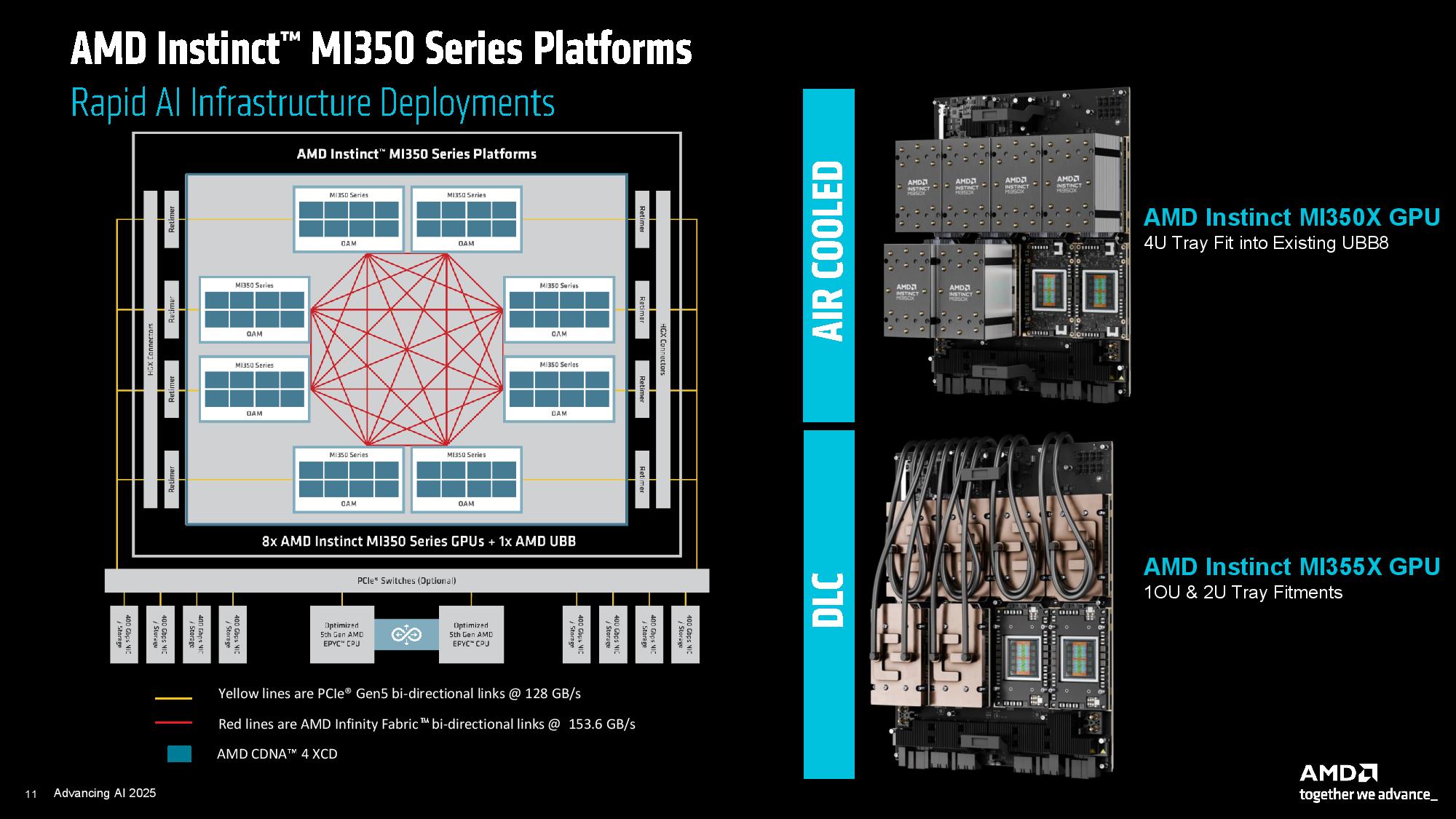
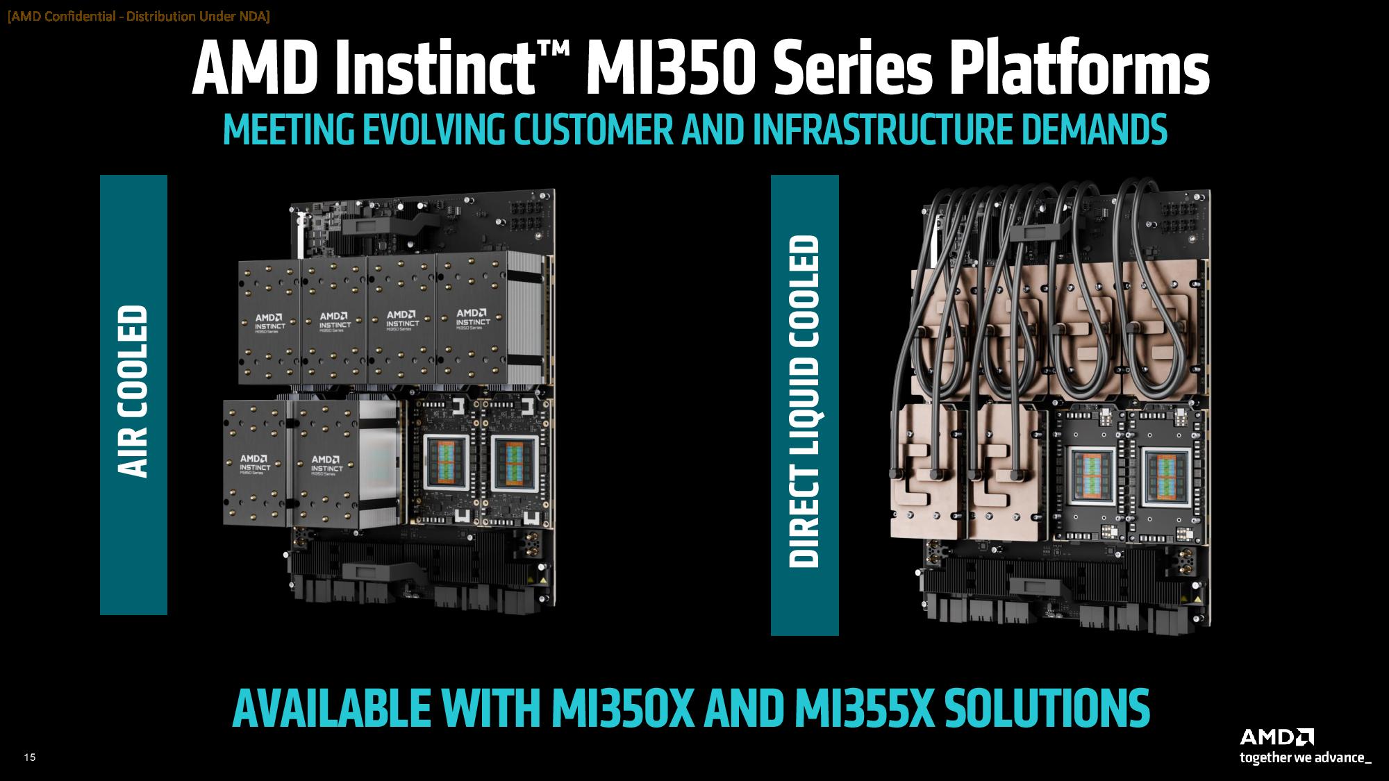
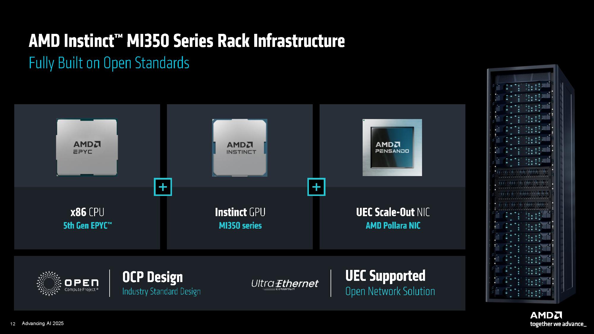
Both the MI350X and MI355X come in an OAM form factor and drop into the standardized UBB form factor servers (OCP spec), the same as prior-gen MI300X. AMD says this speeds time to deployment.
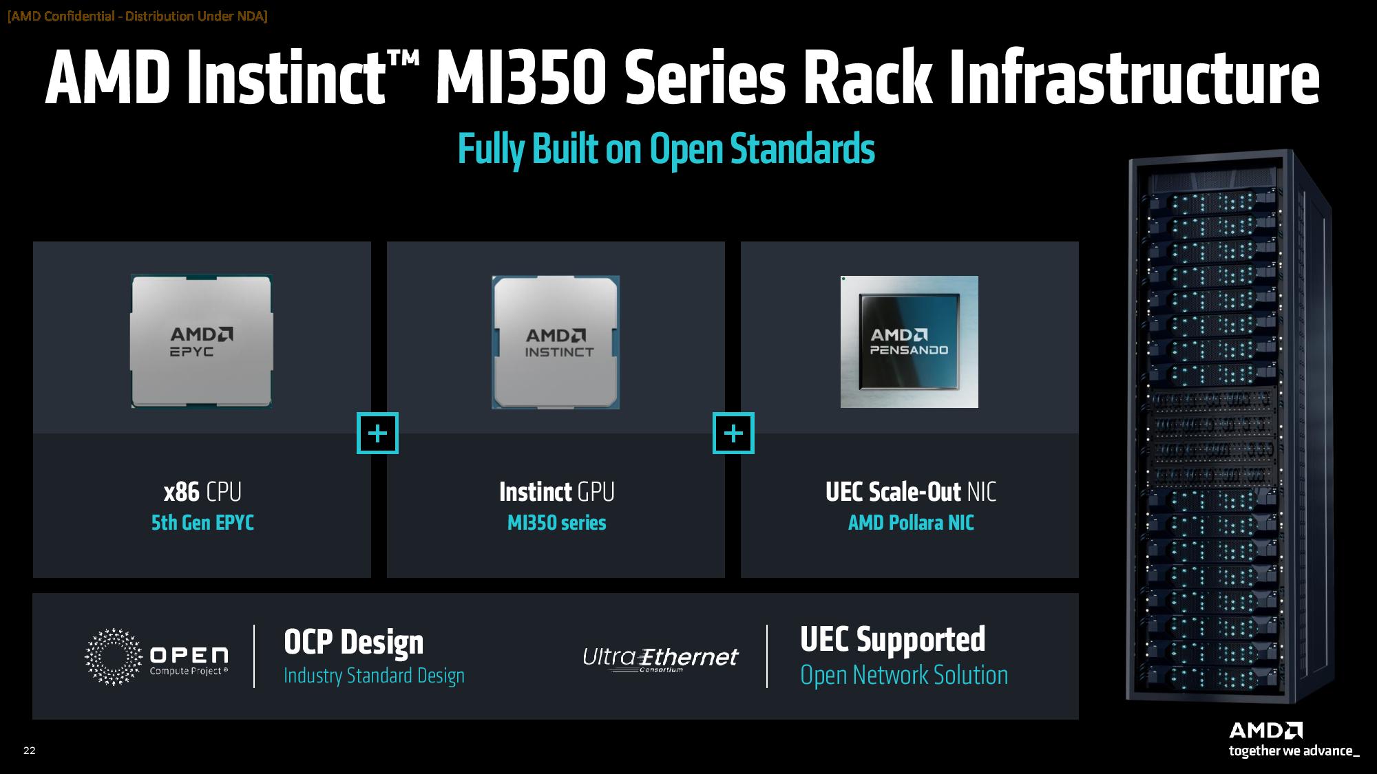
The chips communicate with one another via an all-to-all topology with eight accelerators per node communicating across 153.6 GB/s bi-directional Infinity Fabric links. Each node is powered by two of AMD's fifth-gen EPYC 'Turin' chips.
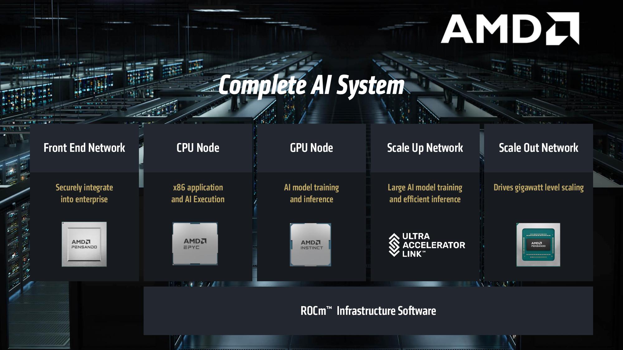
AMD supports all forms of networking, but positions its new Pollara Ultra Ethernet Consortium-capable NICs (UEC) as an optimum scale-out solution, while the Ultra Accelerator Link (UAL) interconnect is employed for scale-up networking.
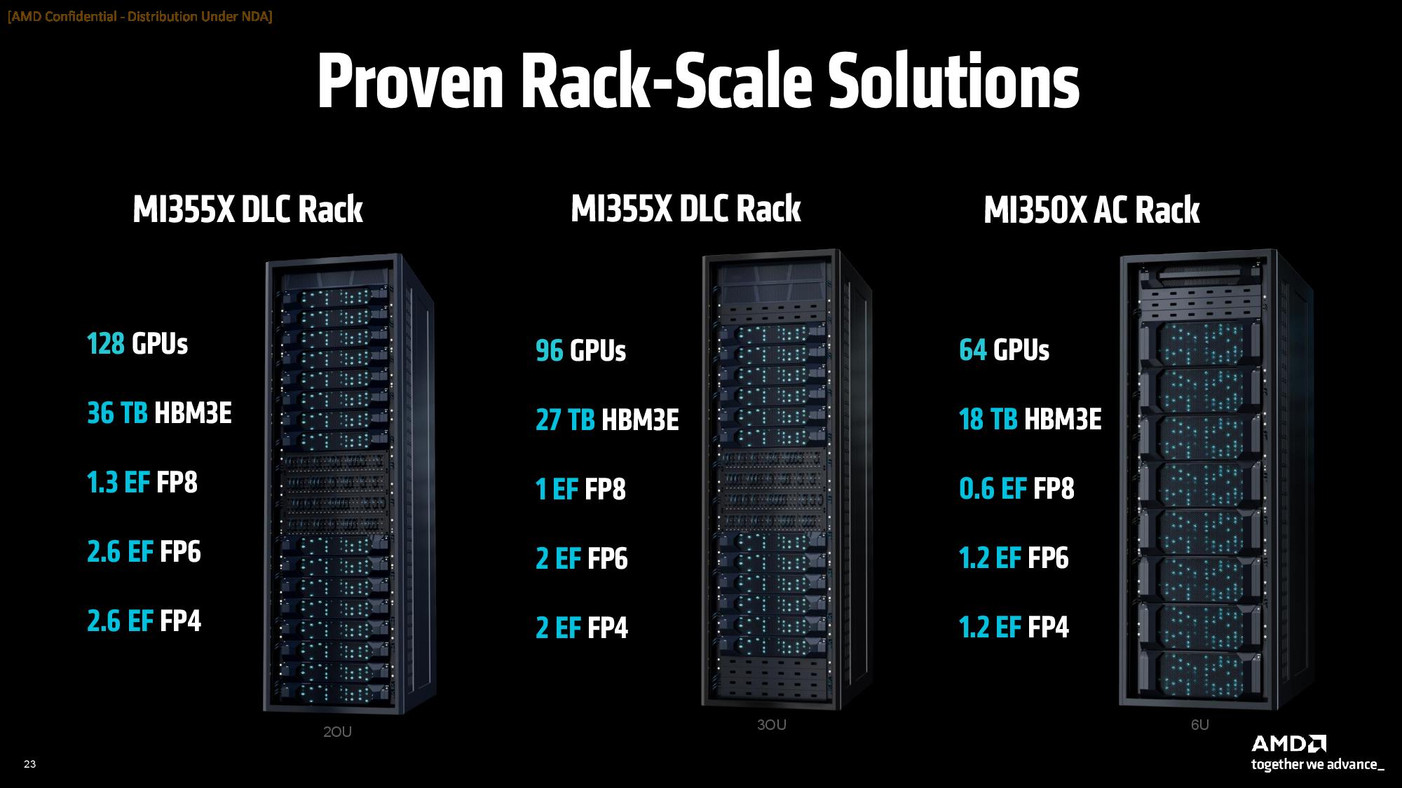
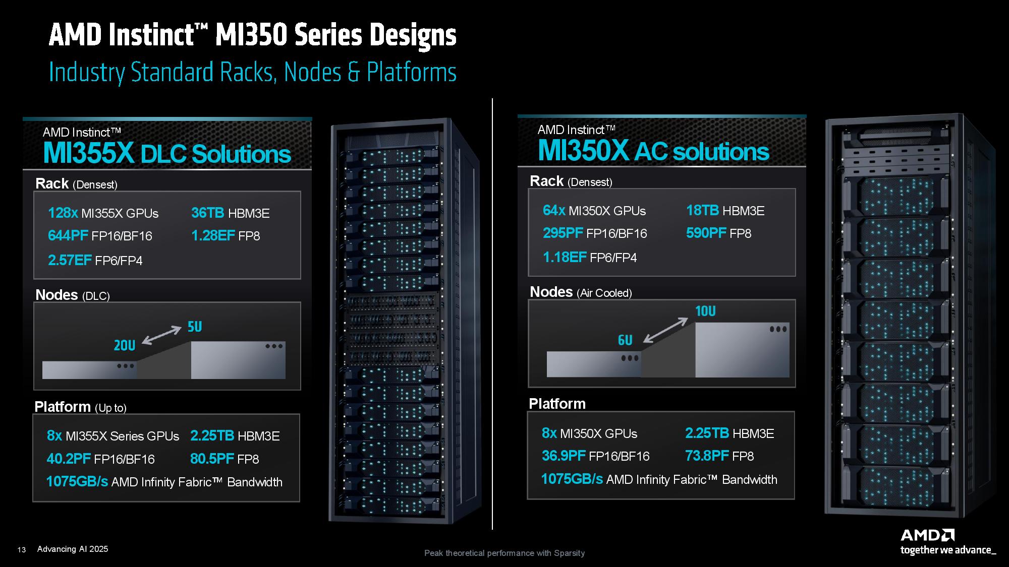
AMD offers both Direct Liquid Cooling (DLC) and Air Cooled (AC) racks. The DLC racks feature 128 MI355X GPUs and 36TB of HBM3E, thanks to the increased density provided by the liquid cooling subsystem, which enables the use of smaller node form factors. The AC solutions top out at 64 GPUs and 18TB of HBM3E, utilizing larger nodes to dissipate the thermal load via air cooling.
AMD has tremendously increased its focus on unleashing the power of rack-scale architectures, a glaring deficiency relative to Nvidia. AMD has undertaken a series of acquisitions and developed a strong and expanding roster of partner OEMs to further its goals.
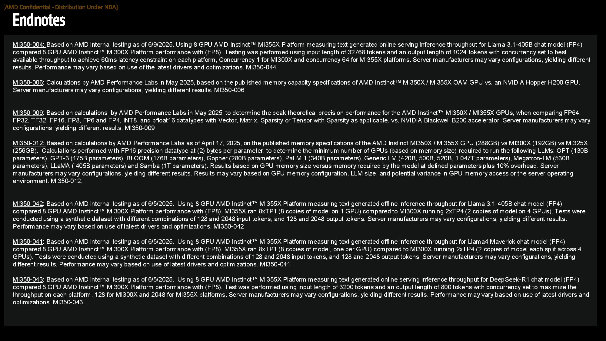
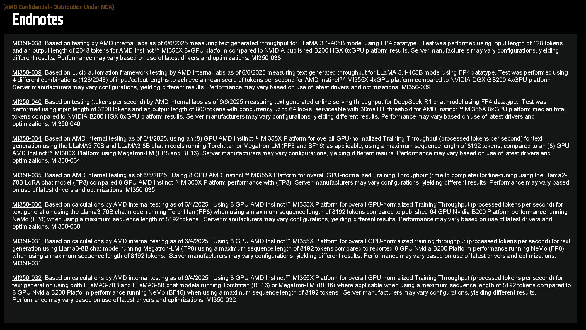
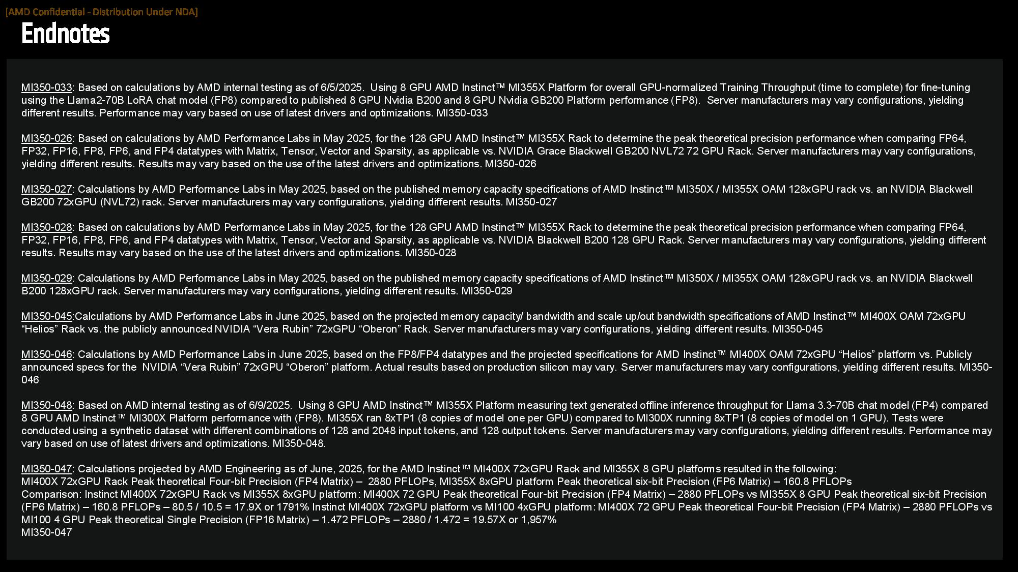
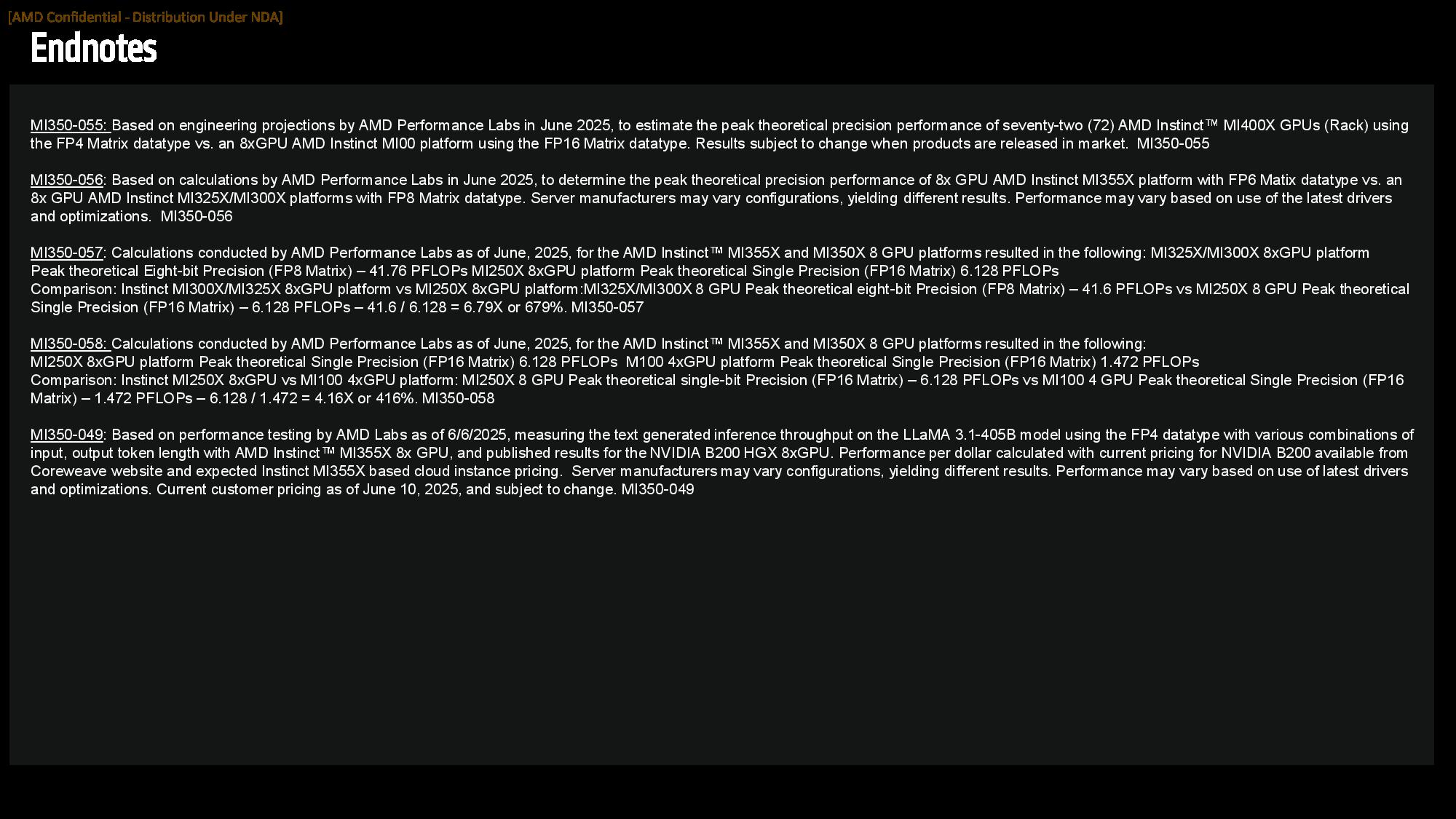
As one would expect, AMD shared some of its performance projections and benchmarks against not only its own prior-gen systems, but also against Nvidia comparables. As always, take vendor-provided benchmarks with a grain of salt. We have included the test notes below for your perusal.
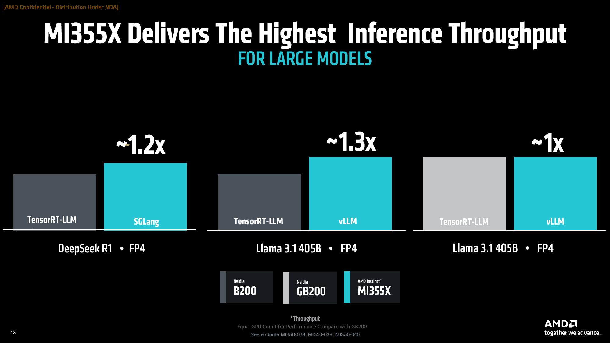
AMD claims an eight-GPU MI355X setup ranges from 1.3X faster with four MI355X vs four DGX GB200 in Llama 3.1 405B, to 1.2X faster with eight MI355X against an eight-GPU B200 HGX config in inference in DeepSeek R1, and equivalent performance in Llama 3.1 405B (all tested at FP4).
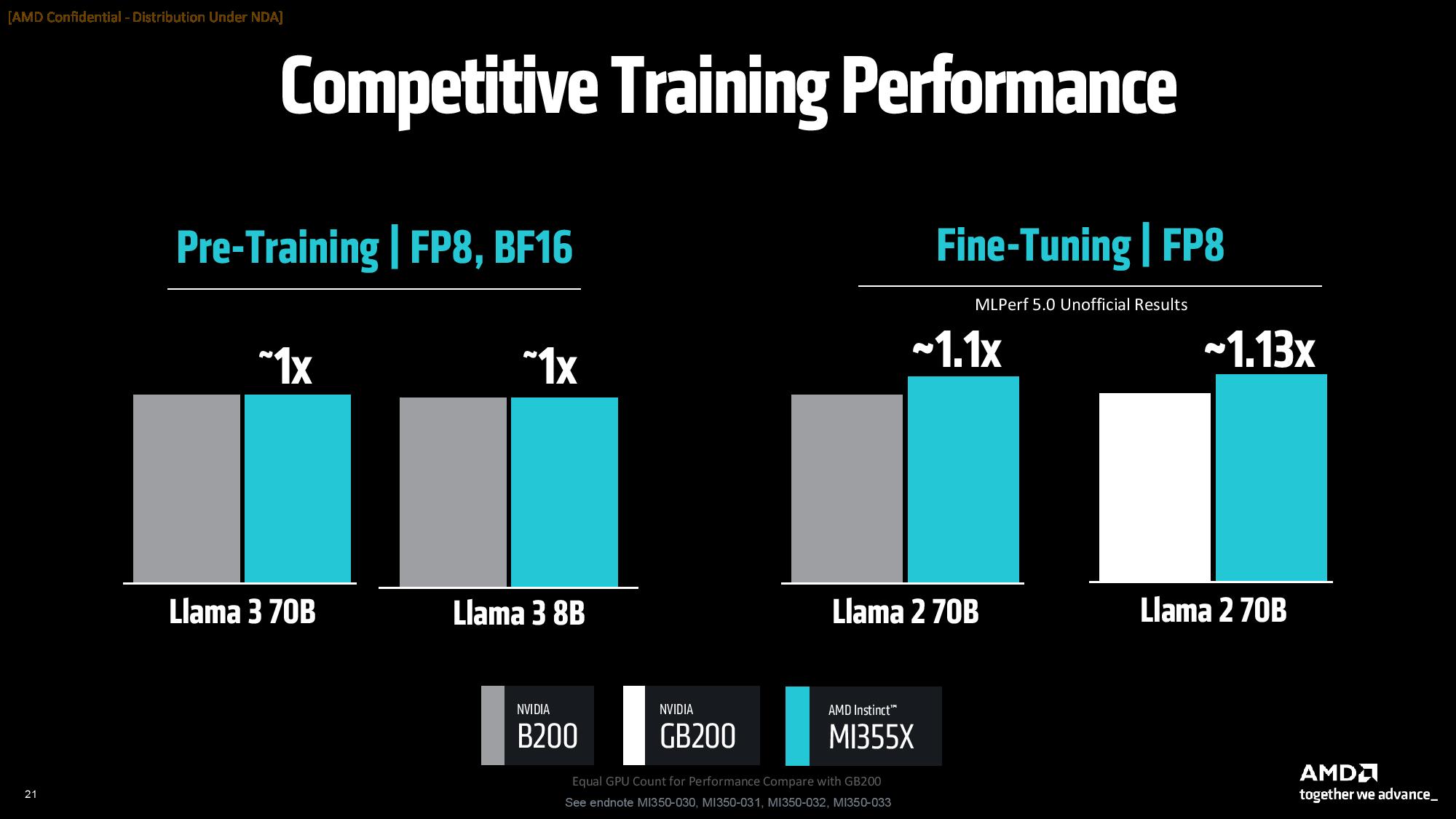
AMD also says MI355X is also competitive with Nvidia's B200 and GB200 in training workloads, though here it highlights either parity or a slight 1.13X performance advantage in a range of LLama models.
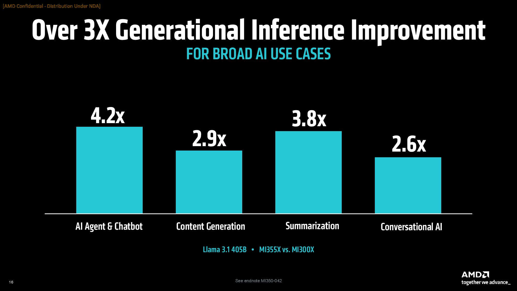
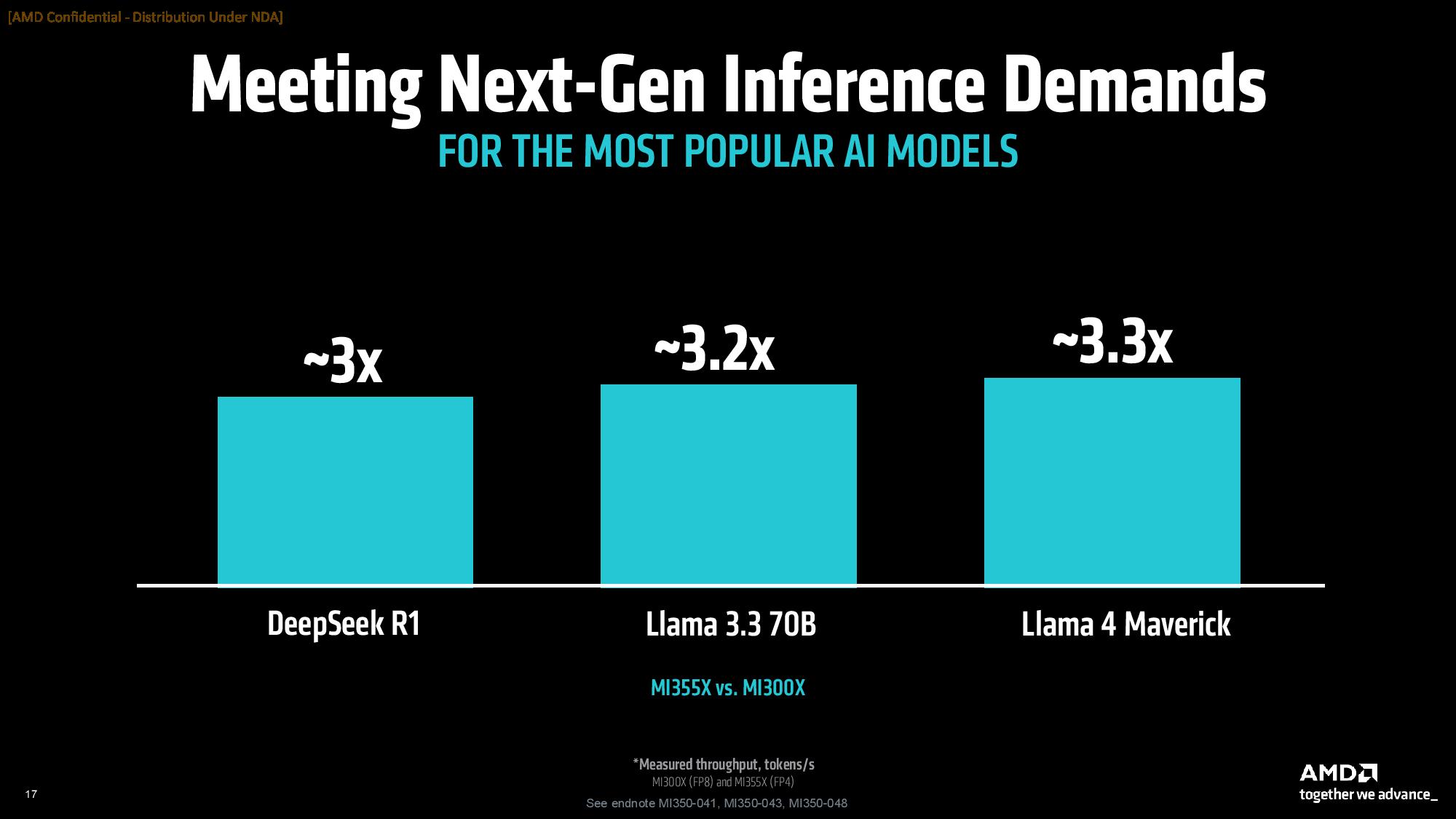
AMD says the MI355X provides up to 4.2X more performance over the MI300X in AI Agent and Chatbot workloads, along with strong gains ranging from 2.6X to 3.8X in content generation, summarization, and conversational AI work. Other generational highlights include a 3X generational improvement in DeepSeek R1 and a 3.3X gain in Llama 4 Maverick.
We will update this article as AMD shares more details during its keynote, which is occurring now.


 English (US) ·